


PCB Fail: Andy bitten by manufacturing defect
Regular readers of this blog will be aware that when I want to get a batch of PCBs made I use the low-cost prototyping services available from the Chinese houses such as Seeed Studio, ITead Studio or Elecrow. It doesn’t really matter which one you choose because I’m convinced that they’re all acting as agents for the same fabrication plant.
Normally when I order these PCBs I specify the 100% e-test option which means that the fab house will run a flying-probe across your pads to check continuity using your Gerber files as a reference.
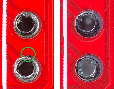
If you look closely at the pads on this 0.5mm pitch QFN you can see the marks that the probe makes in the soft HASL finish.
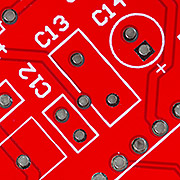
Recently I was working on an exciting new open-hardware project that will be published on this blog in the near future and as usual I received my first batch of prototype PCBs from Elecrow in China. Now, the difference between this and my usual projects is that this one is almost all through-hole, and through-hole boards don’t show evidence of having the e-test. Either the probe that they use is different or they skip the test entirely on the cheap service.
I would normally place the board I was about to work on under the microscope and quickly follow traces and have a look around to make sure everything looked OK. This time I got complacent. Thinking that it’s all through hole, traces are thick, spaces are wide, I’m sure the chances of a manufacturing defect are virtually non-existent.
I was wrong.
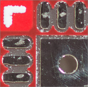
The circled area shows a short between the pad and the plane caused by not enough copper being etched away during the manufacturing process. Of course the pad couldn’t belong to a simple two-pad component such as a resistor or a capacitor. No, it had to be the largest pin-count package on the board. A 28-pin DIP belonging to the ATMega328P on the board.
I didn’t spot the defect while assembling the board. It was only during testing that I noted the GPIO pin appeared to be permanently high. The defect was located under the DIP socket so I couldn’t see it. It was only after probing the line at various points that I determined there had to be a short between that pad and the 3.3V plane on the top of the board. Much sucking of solder ensued using Maplin’s electric desoldering tool. After removing the socket the defect was easily visible.
With the rest of the board populated it made sense for me to fix this on-the-fly by just cutting the short with a stanley knife rather than assembling a completely new board. After putting it all back together everything worked as designed. Phew.
Hopefully this blog entry will serve as a permanent reminder to me about what happens when you get complacent. It only takes five minutes to inspect a new board and a few more minutes to buzz out the traces. Compare that to debugging a new design when you’re not sure if you’ve made a mistake or you’ve got a manufacturing defect and the benefits are obvious.
Pingback: Bitten By PCB Defects | Hackaday()
Pingback: HackFu 2015 – The Badgening | wirewatcher()
Pingback: HackFu 2015 – The Badgening()