


Reverse engineering the Nokia E73 QVGA LCD
Readers with a keen memory will no doubt recall that I said that the N93 would probably be the last of the Nokia QVGA LCDs that I attempt to reverse engineer.
However probably is not definitely and one day whilst browsing ebay my finger slipped and next thing I knew I’d got myself an LCD for a Nokia E73 that was just crying out to be attached to my MCUs. So here we go, another in the series of articles in which I present a low-cost Nokia QVGA LCD that you can use as a display in your own projects.
The E73 LCD
It’s not a blackberry, really!
The E73 LCD is a 2.4″ display that differs slighly from the others that I’ve presented so far in that it’s designed to be used in a landscape (horizontal) aspect whereas the others have been designed to be used in a portrait (vertical) aspect.
All the displays can be put into landscape or portrait mode, the difference is in which direction hardware scrolling is possible. On the E73 hardware scrolling in landscape mode will move up and down. On the others hardware scrolling in portrait mode will move up and down.
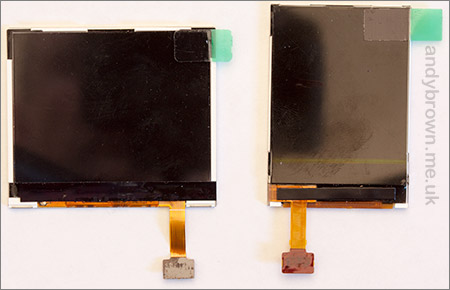
The above image will give you an idea of the relative size and aspect of the E73 LCD (left) compared to the 2.0″ Nokia 6300 LCD (right).
According to the wide variety of sellers on ebay the E73 LCD is also compatible with the E71, E71X, E72 and E63 MS,
The connector
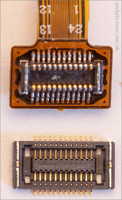
The connector is the same 24-pin JST 24R-JANK-GSAN-TF board-to-board connector made by JST that is used in all the Nokia displays that I have reverse engineered so far.
In previous articles I have linked to JST’s web-shop as a good source for these connectors. However several people have recently written to me saying that JST are now rejecting direct orders for these connectors, giving a reason that they are ‘special connectors for mobile phones’ and directing people to their distributors.
I suspect that JST’s distributors have exclusive sales agreements that would be undermined by the manufacturer offering direct sales and that’s the reason why they are now directing people to them.
The connector is available at very low cost from many resellers, for example:
gsmserver.com
cellnetos.com
stellatech.com
Connector schematic
The schematic for the Nokia E73 is readily available on the internet if you google for it, though, like the others it was probably never intended for release to the general public. Here’s a screen grab of the relevant part that documents the LCD connector.
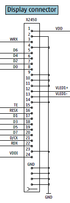
All the usual 8080 bus and control connections are there, as are the LCD backlight circuit in and out connections. As this is a more recent Nokia phone than some of the others there is evidence of refinement to the design such as the elimination of the unnecessary CS input and the single in and out connectors for the backlight array.
Given my previous experience with the other phone models I was not expecting any surprises from this one. So let’s design a schematic for connecting this display to an MCU.
Development board schematic
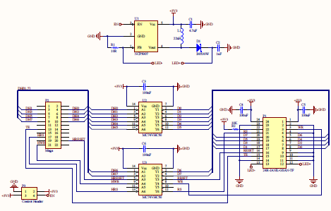
Click to download a PDF of the schematic
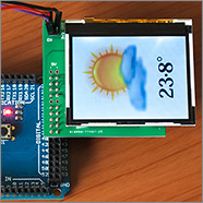
The development board is designed to operate with the Arduino Mega XMEM interface though it will work with any MCU that operates in the 2.8V to 5V voltage range.
There are one or two design improvements since the N93. Most noticeably I have dispensed with the need for a 5V input. It was only ever used to power the backlight boost converter and we can do that with the 3.3V input so in the interests of reducing complexity that’s what I’ve done.
Another improvement is that I’ve routed the TE (Tearing Effect or Vsync) signal out from the LCD to an Arduino pin where it can be used to synchronise writes to the LCD with the display refresh signal to avoid flickering. It’s a CMOS (3.3V) level but should still be enough to trigger an Arduino input high level.
Level conversion
Level conversion is provided by the same pair of OnSemi MC74VHC50 hex buffers that I used successfully in the N93 reverse engineering project.
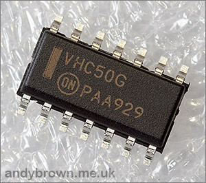
The SOIC-14 footprint with its 1.27mm pin pitch is really easy to work with, positively huge compared to the LCD connector!
Backlight boost circuit
In common with most of the other Nokia LCDs that I’ve reverse engineered this one has a backlight circuit consisting of four white LEDs in series. Assuming a forward voltage of roughly 3.2v for a white LED that means you need around 12.8v to power it.
As in all the previous projects I’ll be using the ever reliable OnSemi constant current LED driver to do the job. It needs only the minimum of external components: an inductor, a schottky diode, a level setting resistor and two capacitors. In return it’ll provide me with a constant 20mA output and an ‘enable’ pin that can be used for PWM dimming.
Bill of Materials
Here’s the complete bill of materials for the schematic.
| Part | Value | Device | Package |
|---|---|---|---|
| P1 | NOKIA12X2 | 24R-JANK-GSAN-TF | 12X2 |
| P2 | pin header | MA12-2 | MA12-2 |
| P3 | pin header | MA2-2 | MA2-2 |
| C1 | 4.7µF | ceramic | 0805 |
| C2 | 1µF | ceramic 50V | 0805 |
| C3,C4,C5,C6 | 100nF | ceramic | 0603 |
| D1 | Diodes Inc. BO530W-7 | schottky | SOD-123 |
| L1 | Sumida 22µH | CDRH5D28NP-220NC | 6x6mm |
| R1 | 10Ω 1% | resistor | 0805 |
| R2 | 33kΩ | resistor | 0805 |
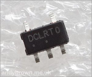
| U1 | NCP5007 | LED driver | SOT23-5 |
| U2,U3 | MC74VHC50DR2G | hex buffer | SOIC-14 |
D1, the schottky diode can be almost any schottky in SOD-123 format. I’ve used the Diodes Inc. BO530W and the ST Micro STPS0520Z interchangeably.
R2 is a pull-up and can take a wide variety of values, 10kΩ all the way up to 100kΩ would probably be fine. I’ve used 33kΩ and 43kΩ with equal success.
The CAD design
After creating the schematic and selecting the footprints for the components then it’s time to create the CAD for the board.
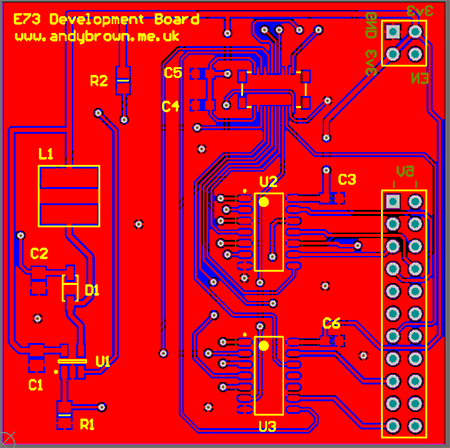
The board was manually routed, I haven’t used an auto-router for some time now because even when they do manage to route to 100% I find some of their routing decisions questionable to say the least.
With hindsight I should have paid more attention to the position of the in/out signals on the level converter IC. There are buffers available that have the in’s and the out’s on opposing sides of the chip which makes routing much easier on a board like this. The footprint that I chose has the in’s and out’s adjacent to each other which means more vias and slightly more complex routing than I could otherwise have got away with.
Building the board
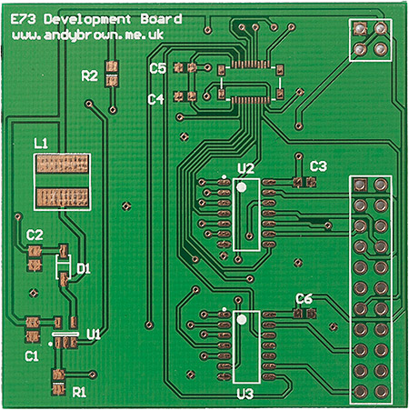
Once I was happy with the CAD I exported the Gerber files and uploaded them to ITead Studio for manufacturing.
About three weeks later the package arrived from China and, as usual, they were perfectly made. I like to think that my designs are conservative and I try to stay well clear of the published limits and tolerances to ensure that I don’t get any nasty surprises when the boards arrive.
My assembly method is essentially unchanged from what I usually do. Firstly all the pads on the board are tinned using a highly active flux, then the board is cleaned of all the flux residue because the acid in the flux would be damaging to the board over the long term. After cleaning I only use water-soluble flux from that point onwards.
The second step is to use a hot plate to reflow the connector, the three ICs and the inductor into place. This step is finalised by touching up the connections with a fine iron under a microscope.
The third step is reflow the remaining SMD components into place with my hot air gun and finally the pin headers are soldered in using a normal iron.
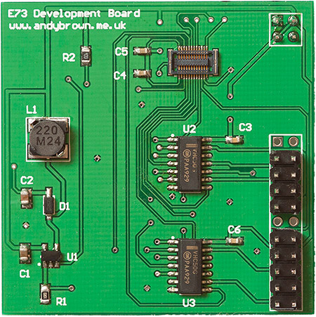
When it’s all assembled I wash the board in hot soapy water, rinse it and leave it to dry for 24 hours.
Software and testing
Before starting any of this I knew it was going to work because I’d prototyped the connections using my generic Nokia hacking board.
With the panel connected to the generic board I was able to make the necessary changes to the Arduino driver software to cater for the differences between this panel and the others.
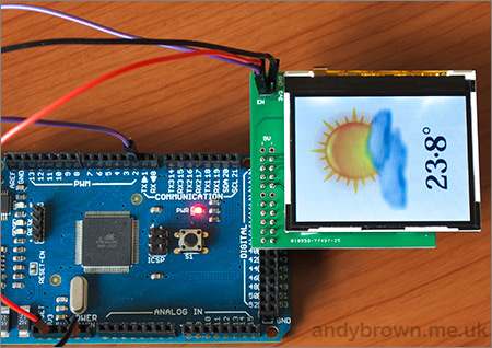
The differences were minimal and were mainly centered around the fact that this panel is normally landscape (320×240 pixels) instead of the portrait (240×320 pixels) mode of all the other screens. It was not hard to adjust my driver code to cope with this without breaking all the other drivers.
I have provided full support for the E73 in my Arduino library, version 2.5.0 and above available from my downloads page. To use the E73 panel you simply need to include its header file and change the name of the declared driver to match the E73.
#include "NokiaE73.h"

using namespace lcd;

typedef NokiaE73_Landscape_262K TftPanel;
Portrait and landscape modes are supported, as is hardware scrolling. I have provided support for 16M, 262K and 64K colour modes although the panels that I have seen so far only support the high-resolution colour modes: 16M and 262K.
Here’s a short, out of focus and poorly lit demo video on YouTube that shows the LCD board in action. Click on the ‘YouTube’ logo at the bottom right to watch it in a larger format at the YouTube site.
Gerbers available
The small number of boards that I had constructed are now all gone but I have uploaded the Gerber CAM files to my downloads page so that you can print your own by uploading the package to a service such as that provided by Seeed Studio, ITead Studio or Elecrow.