Tags
Related Posts
Share This


Project Difficulty

- All components are commonly available.
- There is one QFN integrated circuit.
- The QFN has a 0.5mm pitch with an underside ground pad.
- The smallest discrete component is 0603.
Recent Posts
Exploring the KSZ8091RNA RMII ethernet PHY
In my previous two articles (here, here) I’ve provided schematics and Gerbers for a breakout board that supports the Micrel KSZ8051MLL ethernet PHY. The KSZ8051MLL is an MII PHY manufactured in a reasonably easy to work with 48 pin quad-flat package.
One of the burdens of MII is that it requires rather a lot of pins to implement. The TX/RX data buses are 4-bits wide and operate at 25MHz, allowing the PHY to operate at 100Mb/s.
Enter RMII. RMII is a reduced pin-count interface that multiplexes some of the control and clock signals and halves the bus width to 2-bits at the expense of doubling the clock speed to 50MHz.
The advantage to us is that we can connect an RMII PHY to an MCU without using up so many of our GPIO pins. The main issue we will have is the data and clock rate of 50MHz. We will have to be careful with our board-to-board wiring to ensure that the signals arrive at each end intact.
The Micrel KSZ8091RNA
Micrel’s offering in the low-cost RMII PHY market is the KSZ8091RNA. At only 63 pence in units of 1 from Farnell, it’s very affordable.
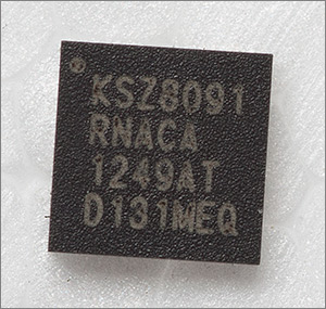
The packaging is a 5x5mm QFN24 with 0.5mm pitch. These leadless packages are major pain in the neck for the hand-solderer’s out there. The edge-pads do have a very small exposure on the sides that mean you could potentially hand solder those but the issue that makes reflow the only viable option is the completely inaccessible center ground pad.
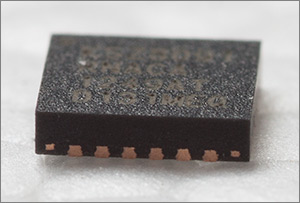
Tiny side pads might make hand soldering possible
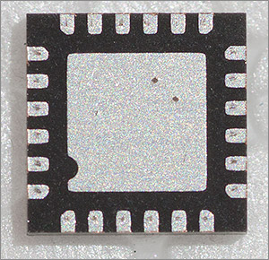
Unfortunately the ground pad cannot be hand soldered
I’ve seen videos where people have attempted to reflow solder through the vias in the PCB pad to make a connection with the ground pad on the QFN. That might work but because you can’t see your work you won’t know if contact has been made.
Looking through the datasheet I can see that Micrel have re-used much of the KSZ8051MLL design in this device which makes it quite simple for me to take my previous design and adapt it to the minor changes. One benefit is that the reduced pin count and size of the QFN means that I have space on the 50mm square board to add some jumpers to select options that the PHY will read when it powers up.
Schematic
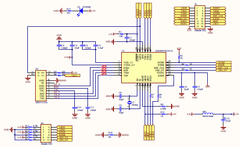
Click for full size PDF
The schematic is a straightforward breakout of the KSZ8091 incorporating an onboard 25MHz crystal oscillator and following the design guidelines for decoupling set out in the datasheet. The P1 header is where the PHY and RMII pins are broken out. The P3 header is where the bootstrap options are set, let’s take a look at those:
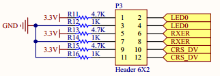
The KXZ8091 has a number of customisable options that can be set at startup by pulling some of the pins low or high. The PHY does contain weak internal pullup/pulldowns on these pins to set default options if you’re not interested in changing them. I’ve opted to break out the option pins to a header that can be used to choose the value of each one.
| Jumper | Function |
|---|---|
| AD0 | PHY is at address 0 (default) |
| AD3 | PHY is at address 3 |
| WoL- | Wake-on-LAN via PME is disabled (default) |
| WoL+ | Wake-on-LAN via PME is enabled |
| 100 | Enable auto-negotiation and set 100Mb/s speed (default) |
| 10 | Disable auto-negotiation and set 10Mb/s speed |
Note that the default address of zero is also the broadcast address for PHYs so if you have multiple PHYs attached to your controller then they’d all respond to this address.
The wake-on-lan options are special feature of the KSZ8091. If enabled, the host MAC can program its address into a PHY register and the PHY will then drive its PME_N2 pin low when it detects the WoL magic packet.
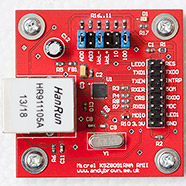
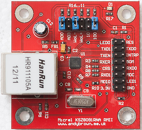
I’ve opted to use the popular and cost effective Hanrun HR911105A ethernet jack in this design.
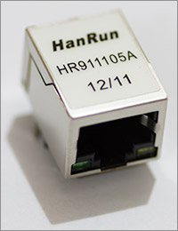
The Hanrun RJ45 connector is easy to get hold of, features onboard LEDs and full magnetics, and tends to be about half the price of competing connectors from other manufacturers.
Board design
I decided to target a 50x50mm square PCB with this design, the idea being that if any of you would like to try to build one of these yourself then you can use the lowest cost service from one of the online manufacturing agents such as Elecrow, Seeed or ITead.
Click for full size PDF
I exported the Gerbers and sent them off to Elecrow for printing. At the time of writing Elecrow offer the coloured soldermask option for free with their $10 for 10 copies service which I think is excellent value. After the usual 3 week wait the boards arrived, and as usual they’re perfectly printed.
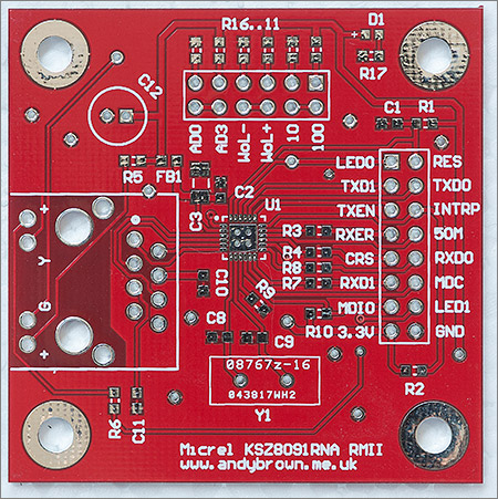
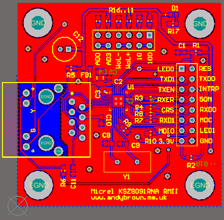
The front of the PCB
As you can see I’ve had plenty of space to include M3 mounting holes. These will be required because there are a few components on the bottom of the board and it’s best to lift these clear of the work surface to avoid the possibility of accidental short circuit.
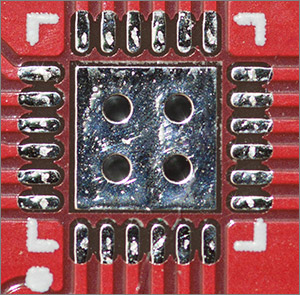
Close up of the QFN footprint
The in-pad vias make the connection with the ground plane on the bottom as well as helping to wick away any heat generated by the IC. You can also clearly see the probe marks in the pads that are made by the ‘e-test’ machine used to test for manufacturing defects. The tolerances offered by the prototyping service don’t permit soldermask between the fine-pitch pins so we do have to be extra-careful when soldering the components to the board.
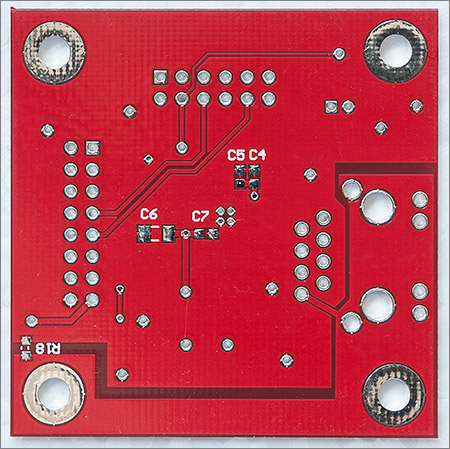
The front of the PCB
The ground plane is split, with the ground for the ethernet jack kept separate from the PHY’s ground. The jack’s ground connects back to the main ground plane via R18, an 0R ‘resistor’, placed very close to the GND pin that goes back to the MCU board.
Assembling the board
My assembly process can be broken down into these steps:
- Apply flux to the top layer pads
- Tin the fluxed pads with a soldering iron.
- Apply more flux to the tinned pads.
- Place all top-layer SMD components on to the tinned pads with tweezers and the assistance of a microscope for the fine-pitch ICs.
- Reflow in my halogen reflow oven.
- Touch up any dodgy connections under the microscope with a soldering iron.
- Solder all the through-hole components with a soldering iron.
- Flip the board over, tin the bottom pads and apply the components with a hot air-gun.
- Wash in warm soapy water, dry overnight and test.
Testing
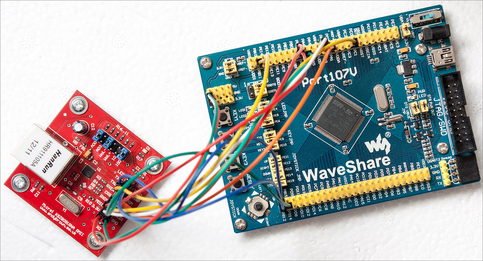
To test the board I hooked it up to an STM32F107VCT6 development board from Waveshare.
Click for larger
If you’ve ever programmed the STM32 before then you’ll know that the pins you can use for the peripherals are not fixed. You can usually choose from a predefined set of pins to avoid clashes and to simplify board layout. The RMII interface is fixed on the STM32F107 but can vary slightly on the F4 as shown in the table below.
| AF11 Function | PHY board label | Normal | Remap (F4) |
|---|---|---|---|
| REFCLK | 50M | PA1 | |
| CRSDV | CRS | PA7 | |
| RXD0 | RXD0 | PC4 | |
| RXD1 | RXD1 | PC5 | |
| TXEN | TXEN | PB11 | PG11 |
| TXD0 | TXD0 | PB12 | PG13 |
| TXD1 | TXD0 | PB13 | PG14 |
| MDC | MDC | PC1 | |
| MDIO | MDIO | PA2 |
As you can see ST haven’t exactly pushed the boat out with the remap options. You can only move the TX pins up from port B to port G, and then only if you’re using at least the 144 pin package. Nonetheless, it’s a welcome option because port B is a crowded place and there’s comparatively little up there in port G. Incidentally, normal and remap are terms that I use based on what they used to be called in the F1 series.
The RXER, LED0, LED1 and INTRP pins are not required in order to get the board working and so they are left unconnected. I have connected the RES (PHY reset) pin to GPIO pin PB14 on the development board.
Naturally I want this PHY to work with the C++ TCP/IP stack included with my stm32plus library. I already support the KSZ8051MLL and so it was a trivial matter to add support for the KSZ8091RNA because they are extremely similar in operation. The device driver code is here on github.
I decided to use my net_udp_send example for the testing. It’ll perform a DHCP transaction to get configuration for itself and then send UDP datagrams to my PC where I can watch for their arrival with Wireshark.
A few modifications need to be made to the network stack configuration before we start. The physical and datalink layers need to be modified to include support for the PHY hard reset on PB14 and the PHY instance itself needs to be changed to the KSZ8091RNA.
template<class TPhy> using MyPhyHardReset=PhyHardReset<TPhy,gpio::PB14>;

typedef PhysicalLayer<KSZ8091RNA,MyPhyHardReset> MyPhysicalLayer;
typedef DatalinkLayer<MyPhysicalLayer,DefaultRmiiInterface,Mac> MyDatalinkLayer;
Secondly, since I’ve configured this PHY to be station zero I need to change the PHY address in the configuration structure:
params.dhcp_hostname="stm32plus";
params.phy_address=0;
That’s it for the essential changes. This example outputs status information to a USART and the default in the example code is Usart3_Remap2 which has a clash with the RMII TXEN pin on PB11 so I change it to Usart1:
typedef Usart1<> MyUsart;
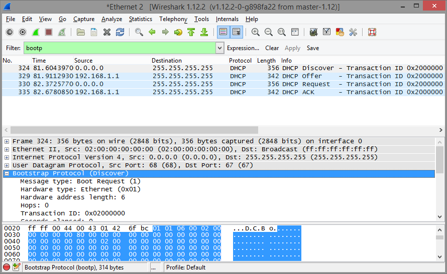
Time to fire it up for testing and thankfully it all worked first time, which is a relief given the difficulty of reflowing the QFN package. DHCP is a broadcast protocol and so Wireshark on my PC was able to capture my network stack performing the DHCP transaction:
Click for larger
Note the default MAC address of 02:00:00:00:00:00. The network stack selects this address as the default if you don’t modify the mac_address member of the Parameters structure.
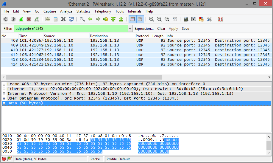
After the DHCP transaction has completed the example goes into a loop sending a batch of UDP datagrams to port 12345 at a configurable IP address every 5 seconds. Wireshark was also able to capture that traffic:
Click for larger
From this I can safely surmise that it’s all working and I’m happy with that. But before I sign off let’s take a look at one more essential topic.
Signal Integrity
No project that features on-board frequencies above a few tens of megahertz is complete without an analysis of signal integrity. This project features cross-board 50MHz signals connected with flying 20cm wires so it’ll be interesting to see just what those signals look like under the oscilloscope.
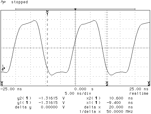
Here’s the REFCLK (50MHz) signal measured at the STM32F107 board pin using my 20 year old 500MHz 1Gs/s HP scope. Not too bad at all actually, and a lot better than I thought it would be. There’s some undershoot and overshoot which is a reminder to me that I probably need to recalibrate and adjust my 10:1 probe rather than any issue with the signal itself.
Download the Gerbers
Fancy building your own board? It’s not that difficult as long as you have the tools to deal with the QFN package. Click here to go to my downloads page where you can find a zip file containing all the Gerber files that an online PCB printing service would require from you. The board size is 50x50mm.
Some boards for sale
I’ve built up a few additional completed boards that are offered for sale here. They’re exactly like in the photographs here in this article and they’re all fully tested using my Port107V board.