


Reverse engineering the Nokia N93 QVGA LCD
Welcome to what will probably be the last in the series of articles in which I reverse engineer one of the Nokia QVGA cellphone displays from the pre-smartphone era. I think that by now I’ve covered every possible aspect of these incredibly cost effective little displays and hopefully opened up new avenues for hobbyists needing a richer display experience than they can get with a simple character LCD.
If you’ve been following these articles then you’ll know that I’ve successfully reverse engineered the 2730, 6300, N82 and N95 8Gb displays. Each one is readily and cheaply available on ebay making them ideal for incorporation into your microcontroller projects. All of my reverse engineering efforts have been accompanied by free, open-source libraries for the Arduino and the STM32.
In this final article I will tackle the N93 2.4″ display, which at the time of writing is available for just a few pounds, dollars or euros on ebay. Let’s see how I get on.
The physical display
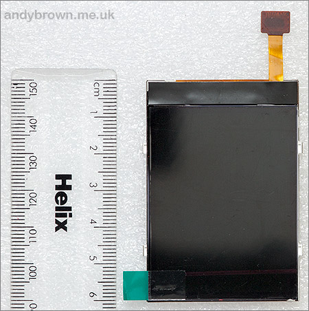
The physical LCD is the same layout as all the previous Nokia LCDs that I’ve tackled. A short FPC cable runs from the LCD and is terminated by a board-to-board connector at the end.
The connector
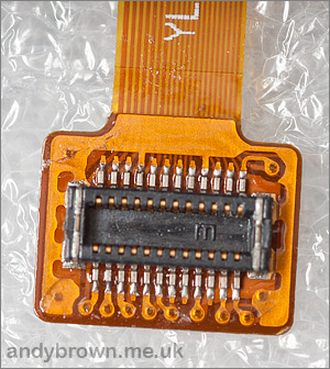
The type of connector is usually a primary source of concern when reverse-engineering a cellphone LCD. Fortunately for me I discovered early on that the 24-pin 0.4mm pitch connector is made by a company called JST. The part number is 24R-JANK-GSAN-TF. Here’s the datasheet.
The connector is readily available in quantity direct from the JST web-store. It’s also available from cellphone repair stores and at the time of writing an enterprising reader is even selling them in single units on ebay.
Determining the connector pinout was not difficult. A little googling quickly unearthed the cellphone repair manual and schematic. Once the LCD connector was located in the schematic it was a simple matter of matching up pins 1..24 with the physical device.
If you look at the photograph of the connector you will see that a number of the pins run directly into a solid plane on the FPC cable. These are the ground connections. With that knowledge it’s trivial to determine where the connector pin 1 is located.
The backlight
I can see from the schematic that the backlight is the same as the 6300 and N82. It consists of 4 white LEDs in series that we must drive ourselves. By far the best way to do this is to use an IC designed to boost voltage and to supply a constant current to the LED string.
We will use the same NCP5007 constant current LED driver from OnSemi that we’ve been using in all our Nokia TFT designs so far. It’s cheap, simple to configure and requires few external components to make it work.
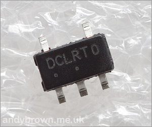
The NCP5007 will be configured to supply a constant 20mA through the backlight circuit and we will use a PWM signal on the ENABLE pin to vary the brightness.
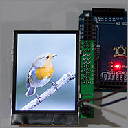
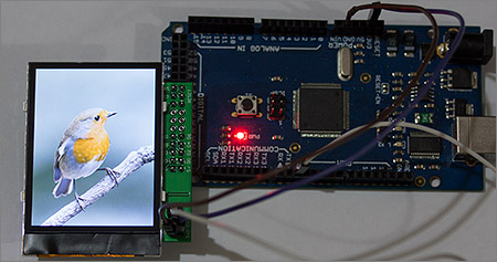
An Arduino development board
It’s become something of a tradition for me to prove the reverse engineering by designing a development board for the Arduino Mega and I’ll continue that tradition here.
Level Conversion
All my previous boards have featured level conversion using the NXP 74ALVC164245DL device. We need level conversion because the Arduino Mega has 5V GPIO levels and I have to assume that these screens are designed for a maximum of around 3.3V. I’ve lost count of the number of TFT controller datasheets that I’ve read and I’ve never yet seen one that is designed for 5V I/O.
For this board I decided to use a different method of level conversion using a pair of logic buffer ICs. The device I use is the MC74VHC50 hex buffer from OnSemi, and I need two of them to handle all the signals on the board.
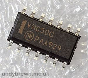
These ICs have 5V-tolerant inputs and a variable output determined by its VCC pin. The reason for this change in design is that these logic ICs are easier to get hold of, cheaper to buy and slightly easier to work with due to the wider pin pitch.
Before producing the LCD development board I verified that the level conversion strategy would work by hacking up some wires to the leads of the IC and verifying that an input level of 5V would be correctly converted down to 3.3V.
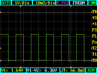
The image from my little pocket oscilloscope shows that the test square wave is perfectly reproduced on the IC output pin. You’ll have to take my word for it that the level is 3.3V in that image.
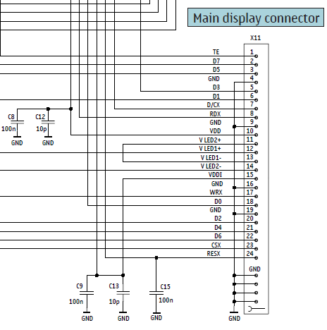
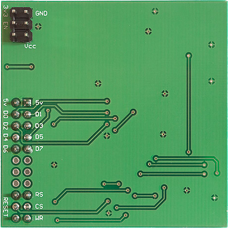
Schematic
The schematic image shows the display connector, level converter, backlight circuit and arduino connector all linked together. I decided to add a small amount of capacitance to the active-low RESET line to enhance its stability. I’ve never seen any unexpected resets in any of my boards but I note that all the official Nokia schematics add capacitance here so I’ve followed suit this time.
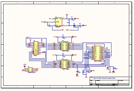
Click on this thumbnail for the schematic PDF
Here’s the complete bill of materials for this schematic.
| Part | Value | Device | Package |
|---|---|---|---|
| P1 | NOKIA12X2 | 24R-JANK-GSAN-TF | 12X2 |
| P2 | pin header | MA12-2 | MA12-2 |
| P3 | pin header | MA3-2 | MA3-2 |
| C1 | 4.7µF | ceramic | 0805 |
| C2 | 1µF | ceramic 50V | 0805 |
| C3,C4,C5,C6 | 100nF | ceramic | 0603 |
| C7 | 22pF | ceramic | 0603 |
| D1 | Diodes Inc. BO530W-7 | schottky | SOD-123 |
| L1 | Sumida 22µH | CDRH5D28NP-220NC | 6x6mm |
| R1 | 10Ω 1% | resistor | 0805 |
| R2 | 33kΩ | resistor | 0805 |
| U1 | NCP5007 | LED driver | SOT23-5 |
| U2,U3 | MC74VHC50DR2G | hex buffer | SOIC-14 |
PCB layout
After designing the schematic the next step is to lay out the printed circuit board and route the traces between the components. My target board size is 50x50mm square so that I can use the cost-effective manufacturing service provided by ITead studios in China.
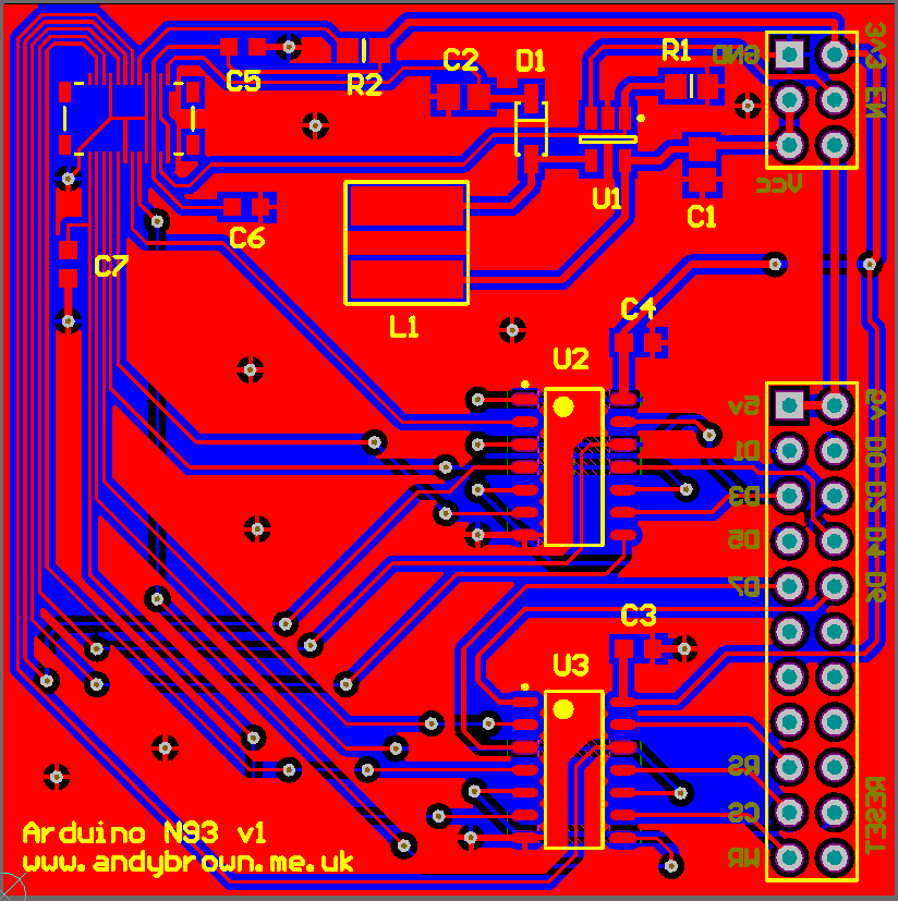
The most critical part of this layout is the positioning of the LCD connector. It has to be accurately placed so that the LCD, when connected, wraps around the board and sits perfectly on the other side mounted on double-sided sticky pads to lift it clear of the board traces. In the above image pin 1 of the LCD connector is down the bottom right.
As usual these days I don’t even consider the auto-router built in to the design package. Manual routing is time consuming but the results are always better than an auto-router.
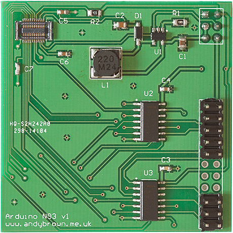
When the design was completed to my satisfaction I generated the Gerber files and sent them off to ITead for manufacturing. About two weeks later they arrived.
![]()
![]()
As usual the boards from ITead are flawless and I can get started with the build. My process is essentially unchanged from what I usually do. After tinning the contacts on the board I place the difficult components (the ICs, the connector and the inductor) with the aid of some flux and bake them on a hot plate. The solder on the tinned pads melts and the components drop into place.
The remaining discrete components are much easier to handle and I simply reflow them into place using my hot air gun and a pair of fine tweezers. When all is complete I examine the results under my binocular microscope and finally wash the boards to remove excess flux.
Testing the board
Only now, several weeks after starting do I get to see if the whole thing works. I’m hopeful though, given the success of the previous reverse-engineering efforts.
I quickly determined that the LCD controller is much the same as the 2730, 6300 and N82 with only minor differences around the commands that control the orientation. We don’t really know the official identity of this controller but it’s close enough to the MagnaChip MC2PA8201 that we can work from its datasheet with a high degree of confidence.
Even better, this batch of screens that I got on ebay appears to be of a very high quality. They’re bright, the colours are accurate and the viewing angle is very wide. They were advertised as ‘genuine Nokia’ and certainly appear to perform as if that’s what they are.
It’s not all plain sailing though. Despite my best efforts I’ve not managed to discover the correct sequence to do vertical scrolling. If any Nokia engineers are out there reading this and want to anonymously drop me a tip then my contact form awaits your keystrokes. Go on…
I have provided full support for the N93 in my Arduino library, version 2.4.0 and above available from my downloads page. To use the N93 panel you simply need to include its header file and change the name of the declared driver to match the N93.
#include "NokiaN93.h"

using namespace lcd;

typedef NokiaN93_Portrait_262K TftPanel;
All the examples except those that feature hardware scrolling such as the terminal demo are supported. The panels that I have obtained on ebay all support 16M and 262K colour modes in portrait and landscape orientation. Driver support is provided for the 64K colour mode but the panels that I have obtained don’t support it.
Here’s a short demo video on YouTube that shows the LCD board in action. Click on the ‘YouTube’ logo at the bottom right to watch it in a larger format at the YouTube site.
Gerbers available
I’m afraid that the additional boards that I built have now all gone but I’ve now made the Gerber CAM files available from my downloads page so you can get your own printed simply by uploading the package to a service such as Seeed Studio, ITead Studio or Elecrow.