Tags
Related Posts
Share This


Project Difficulty

Recent Posts
Bluetooth Low Energy and the STM32WB55 MCU
I’m a subscriber to ST’s regular email newsletter and though most of it isn’t interesting to me I did notice that in one of the recent editions they were promoting their wireless range of STM32-based MCUs. As a big fan of the STM32 this caught my eye and co-incided with some ideas that were spinning around in my head for new wireless projects.
The series of MCUs in question is the SMT32WB55 and so I went off to familiarise myself with what ST were offering.
It turns out that these are very flexible wireless devices. Operating in the 2.4GHz range they are capable of implementing any protocol that ST has decided to provide a wireless stack for, which at the time of writing includes BLE, Bluetooth Mesh, Zigbee and Thread.
The cost of this flexibility is ease of use. These ICs do not provide a simple high-level programming interface that hides the underlying protocols from you. They’re very much like the ST USB peripheral — flexible but expect to get your hands dirty with the details of the protocol. If you’ve ever seen ST’s low-level source code before then you will be feeling a sense of foreboding right about now.
Challenge accepted, as they say on the internet. I set about designing a board that would allow me to experiment with BLE in the form of a wireless, battery-powered temperature sensor. After all, all this RF stuff can’t really be as hard as they say it is; can it? Actually yes, it is. But more on that later.
The wireless temperature sensor design
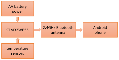
I decided to support four NTC thermistor-type sensors, each one providing an input to one of the STM32 ADC channels through a simple resistor divider that would allow me to easily calculate the temperature by way of an accurate external reference voltage provided to the MCU.
The MCU will be battery-powered direct and unregulated from two AA cells so I’ll need to be aware that the input voltage level will fluctuate from betwen 3.2V down to around 2V when the cells are exhausted. Running from battery power means that I’ll need to be mindful of power consumption. My target battery life will be a week from a pair of rechargeable AAs that will only have about 2.5V when fully charged.
The big variable is BLE itself. I’ve never worked with the protocol before and have only downloaded and skimmed the ST documentation. What I’m planning seems feasible and it’ll be this project that validates that. Even if I run into a brick wall I will have learned a lot along the way.
Off we go then, here’s the schematic that I’ll be building.
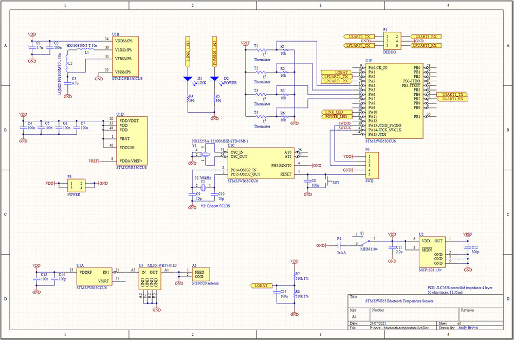
Click on the thumbnail for a full-size PDF.
Not very much to it is there? It’s basically just the MCU, temperature sensors, voltage reference and the RF antenna. Oh yes and a couple of LEDs to flash for fun.
The voltage reference
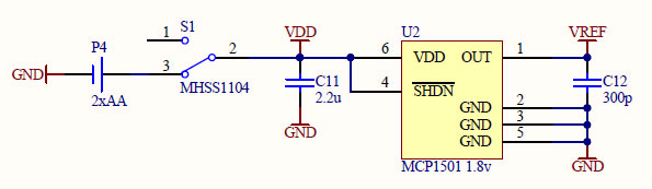
Since I’m going to be using the ADC I need a steady reference voltage. My battery supply will run from about 3.2V for non-rechargeable AAs down to 2V so my selection of reference voltage is 1.8V, provided by a Microchip MCP1501.
The STM32WB55
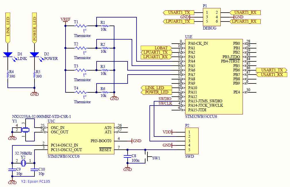
The schematic for the MCU follows ST’s recommendations. The maximum clock speed for the MCU is 64MHz and to that end there’s a 32MHz crystal on the board. I will actually run the CPU clock slower than 64MHz to save battery power. ST’s software stack requires a low speed clock and so I’ve provided a 32.768kHz crystal for the LSE. The SWDIO and SWCLK lines provide the programming and debug interface.
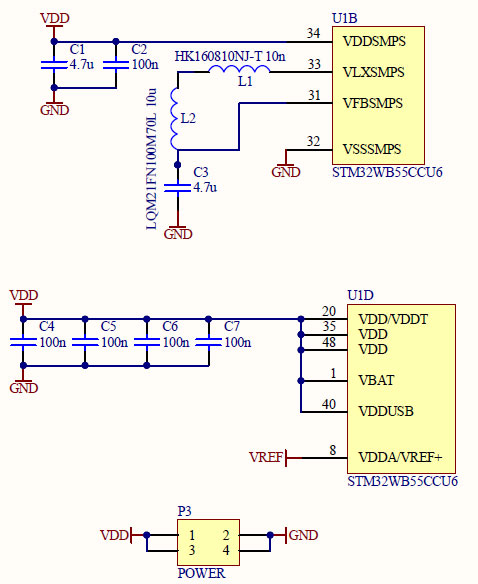
The power supply setup is a little different to what you might be used to with an STM32. To reduce power consumption there’s an efficient switch-mode power supply on the die and you have to provide external inductors for it. The values are given in the datasheet and are provided by me in the above schematic. The SMPS switches itself out in favour of the LDO when the MCU voltage falls below a certain level.
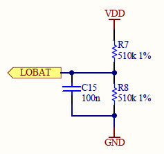
It makes sense to have an input that will tell me when my battery is going flat so I’m doing that with a simple voltage divider tapped at the center to an ADC input on the MCU. A full 3.2V charge will measure 1.6V at the ADC, falling to 1V as the battery life is exhausted.
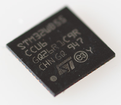
A very flat QFN
The MCU is not offered in a package that has leads, presumably to avoid creating antennas where they should not be. The most hacker-friendly package is the QFN48 in the 256kB STM32WB55CCU6 MCU. This is the thinnest QFN I’ve seen to-date. Even the 0603 capacitors tower over it. The market for slimmer and slimmer smart devices is driving IC manufacturers to produce ever more compact packages.
The QFN has an exposed ground pad on the bottom, and it’s the only ground connection so it has to be soldered down. This is the only part of working with a QFN that I dislike. In fact I dislike any package pin where I can’t get a probe in to test continuity after the board has been made.
The temperature sensors
These sensors are simply NTC thermistors that you can get on ebay. Technically speaking they are a 3950 NTC with a beta value of 3380, a nominal resistance of 10k@25C and a dissipation constant of 5mW/C. These values are important when it comes to implementing the conversion software later on.
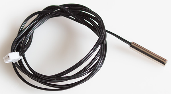
By placing them in the upper section of a potential divider with a known lower section I can tap off the center to an ADC input, measure the voltage and hence calculate the resistance of the thermistor and from that I can calculate the temperature (more on that below).
Accurate readings depend on the stability of the discrete resistors over time and temperature. It doesn’t matter so much if they’re a 1% or 5% value tolerance because you can get your most accurate multimeter out and measure them before soldering them to the board then the software can be programmed to use the measured values — and that’s exactly what I did.
The Antenna
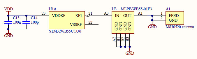
ST have written application notes that provide you with many antenna options. AN5129 explains PCB-printed antennas and provides reference designs and AN5434 goes into even more detail. I’m certainly not short of options. My first attempt was an abject failure but we’ll save my cock-ups for later in this article. This new, improved version uses an Ethertronics M830520 2.4GHz chip antenna filtered by an ST MLPF-WB55-01E3 passive filter network.
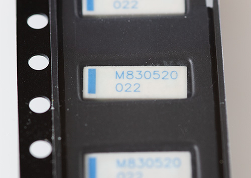
Ceramic chip antenna
I really need to talk about that filter IC. It is a tiny, microscopically small, bumpless 6-pad chip-scale IC. It is by far the smallest package I’ve ever had the displeasure to work with. It is, however, a beautiful thing to behold when viewed under the microscope. My microscope is a traditional design that you look into with your eyes and doesn’t have a camera attachment so I couldn’t capture an image that way. This is the best image I could take using a DSLR with a 2:1 macro lens setup.
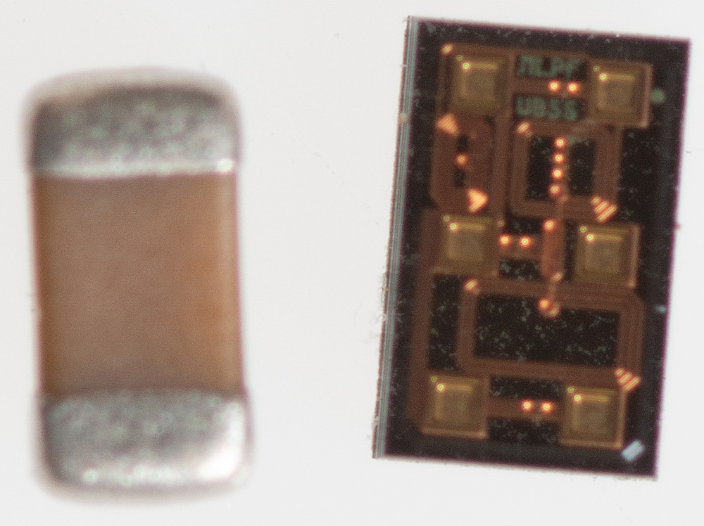
An 0603 capacitor is included for reference
It is made entirely from glass with a black top and the filter network etched on by some sort of laser or other extremely high-precision manufacturing process. The 6 tiny pads that you can see are on the outer surface of the glass and the connecting network is at least one layer of glass below it. Writing the product code in there in a 100µm font is just showing off.
And I thought working with the QFN was going to be a pain.
Bill of materials
Here’s a full bill of materials for this project.
| Identifiers | Value | Quantity | Description | Footprint |
|---|---|---|---|---|
| C1, C3 | 4.7µ | 2 | Ceramic capacitors | 0603 |
| C2, C4, C5, C6 C7 | 100n | 5 | Ceramic capacitors | 0603 |
| C9, C10 | 10p | 2 | Ceramic capacitors | 0603 |
| C11 | 2.2µ | 1 | Ceramic capacitors | 0603 |
| C12 | 300p | 1 | Ceramic capacitors | 0603 |
| C14 | 100p | 1 | Ceramic capacitors | 0603 |
| D1 | Link LED | 1 | Red LED | 2012 |
| D2 | Power LED | 1 | Red LED | 2012 |
| L1 | 10n | 1 | HK160810NJ-T inductor | 0603 |
| L2 | 10µ | 1 | LQM21FN100M70L | 0805 |
| P1 | HDR2x3 | 1 | 2x3-pin header | 100 mil |
| P2 | JST XHP-5 | 1 | Female SWD header | 5x 2.5mm |
| P3 | HDR2x2 | 1 | 2x2 pin header | 100 mil |
| P4 | 2xAA battery holder | 1 | Keystone Electronics 2462 | custom |
| R1, R2, R3, R6 | 10k | 4 | SMD resistor | 0805 |
| R4, R5 | 390 | 2 | SMD resistor | 0805 |
| R7, R8 | 510k 1% | 2 | SMD resistor | 0805 |
| S1 | power switch | 1 | MHSS1104 | custom |
| SW1 | reset | 1 | PCB pushbutton | custom |
| T1, T2, T3, T4 | JST XHP-2 | 4 | thermistor connectors | 2x 2.5mm |
| U1 | STM32WB55CCU6 | 1 | MCU | UFQFPN-48 |
| U2 | MCP1501 1.8v | 1 | Microchip voltage reference | SOT23-6 |
| U3 | MLPF-WB55-01E3 | 1 | Passive filter network | custom |
| Y1 | NX3225SA-32.000MHZ-STD-CSR-1 | 1 | 32MHz crystal | custom |
| Y2 | Epson FC135 | 1 | 32.768kHz crystal | 2012 |
PCB layout
Four-layer impedance-controlled PCBs for $6 from JLCPCB are now the new normal so of course with this being a project that has a gigahertz RF component that’s the stackup that I chose to use. The inner layers are unbroken ground and power, respectively.
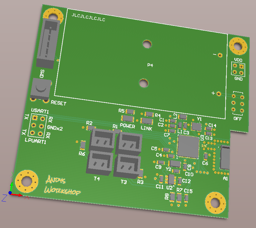
The trace leading to the chip antenna is 11.55 mil that makes it 50Ω impedance. The layout for the chip antenna is taken directly from the Ethertronics datasheet and of course the inner and bottom layers are stripped of copper beneath it. The biggest worry I had was whether the tiny 300µm pads for the MLPF filter would prove too much for the $6 manufacturing process.
PCB Manufacturing
I never bother with the expensive express delivery options and so it took a couple of weeks for my pack of 5 PCBs to arrive from JLPCB. Here they are.
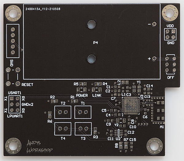
Thankfully there were no problems with the MLPF pads and the soldermask inbetween them was intact. Most, but not all of the soldermask was intact between the QFN pads as well which will help a little with the construction.
I rather like the new-style black soldermask that JLPCB are using. To my eyes it looks rather smart and most importantly you can see the traces. The old style glossy black soldermask was much heavier in appearance and completely obscured the traces.
I went ahead and built the board by tinning the pads, balancing the components on the little solder bumps and then running the board through a reflow cycle in my reflow oven. Getting solder on to the QFN ground pad took some effort because of the heatsink effect of the inner ground plane. I had to use simultaneously use a heat gun to heat the whole area and a soldering iron to flow the solder out across the pad.
Board testing
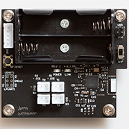
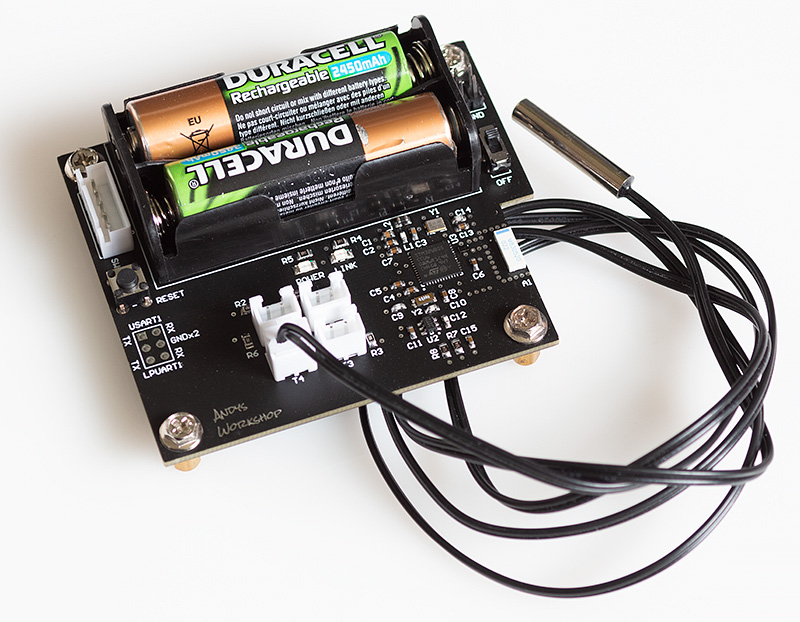
Here’s a picture of the board half-built with enough components for me to be able to test that it’s functioning. There’s no point wasting components if the board proves to be a write-off. All the firmware design and test was done with the board in this skeleton state.
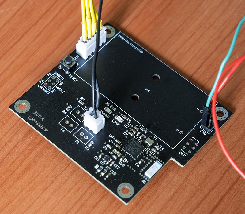
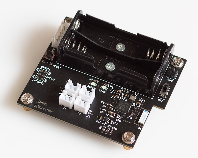
Once tested the board can be fully assembled with the remaining components. Now it’s starting to really look the business.
Let’s talk about failure
I’ll let you into a little secret. This isn’t my first attempt at this board. My first attempt was a couple of months ago and it looked like this:
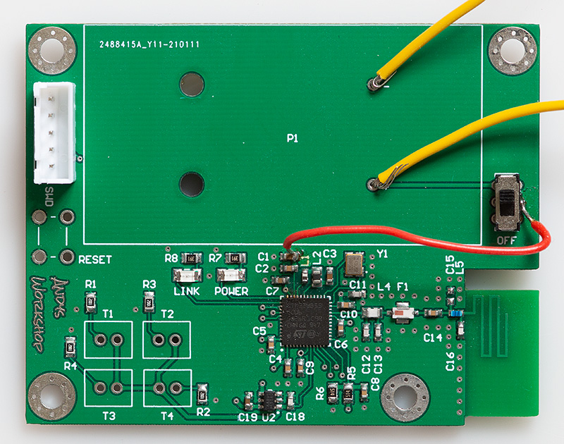
A number of things went wrong with this board that, when taken together made it obvious that I’d have to go back and revise the design for a version 2.
The footprint for the battery holder was wrong. Somehow I’d managed to mis-read the datasheet and place the mounting and terminal holes offset to the left. I blame the technical diagram. Honestly, I think there’s a competition going on between the guys that draw those diagrams to complete them with the fewest number of labelled distances leaving you to get a calculator out to work out the key offsets and sizes!
Secondly, and more seriously I’d forgotten to hook up the MCUs VDD net on the schematic to the battery output. That red bodge-wire that you see was put in place to work around that fail. Major facepalm.
Thirdly, I’d forgotten to provide some pins for external power input. Although this design was going to be battery powered I would need pins to provide power from my bench PSU during testing and development. Those yellow bodge wires that you see are working around that omission.
By now I was wondering whether it was possible to get anything else wrong with the design, and of course the answer was yes it was possible. In this first version I’d decided to go with a PCB meandering printed antenna. The dimensions were strictly copied from an ST application note and the associated passive filter network also taken from their application note.
It didn’t work. It simply didn’t show up at all on my smartphone bluetooth monitoring apps. Without a VNA on my bench there was no way I could even attempt a bodge so it was at this point that I had to give up and create version two.
Version two, the black one, fixes all the issues and adds pin headers for the USART/LPUART peripheral because I noticed that the ST code uses those for debug output and they could prove useful. As you’ve seen by now I’ve also abandoned my attempts at a printed antenna and filter network based on discrete components in favour of a chip antenna and filter IC.
Testing version two
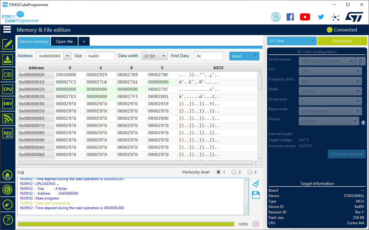
I hooked up my ST-Link, connected external power and switched on. My Windows desktop ST-Link application detected that there was something there but refused to ID it which was slightly worrying. After a bit of Googling it turns out that these STM32WB55 devices are a bit strange and will only be detected by the STM32CubeProgrammer application. This is a cross-platform java application that will work fine on Windows but on Linux its dependency on an old javaFX library means that it won’t work with the latest OpenJDK releases. On Linux I’ll be using the command line interface anyway, and on Windows the GUI looks like this:
Programming the STM32WB55
This is not as simple as just plugging in your ST-Link and flashing your masterpiece to the onboard flash memory. There are two processors inside this device, three distinct firmwares and multiple areas of flash and SRAM, some of which are shared between the CPUs and some of which are protected.
The main CPU onboard is a Cortex-M4 running at up to 64MHz. The co-processor that you cannot access directly is a Cortex-M0+ running at 32MHz. This CPU runs the RF firmware stack that you upload. The WB55 SKU that I’ve selected comes with 256kB of flash and 512kB and 1MB devices are available. 256kB of flash and 128kB of SRAM may seem like a lot but the RF firmware stack will take a significant bite out of both the flash and SRAM so you may need to buy a larger device than you think you need.
The three firmwares on this device are:
- A firmware upgrade service used to upgrade the wireless stack. This is known as the FUS.
- The wireless stack.
- Your application firmware.
Updating any firmware requires you to use the STM32CubeProgrammer utility. The normal ST-Link utility will not recognise the WB devices — something that caused me to think my board was dead until discovering this little nugget of information on the internet.
Speaking of things you don’t easily find in ST documentation; the SRAM memory cannot be read back over the SWD connection and will always return 0x0000000 so when you see forum posts and documentation telling you to check the content of an SRAM location then forget it, you can’t. Only boards that have a USB programming connection can read out the SRAM.
The Firmware Upgrade Service (FUS)
This is the first firmware that you’ll have to tackle before you can do anything else. All STM32WB55 devices come with version 0.5.3 of the FUS installed and it must be upgraded before you can do anything else. At the time of writing version 1.2.0 is the latest version and it is (theoretically) possible to directly upgrade to it. Previously you had to step up the versions to get to the one you want.
Once upgraded, the FUS cannot be downgraded.
Application note AN5185 is the place to start when researching which versions of the FUS are available and what your upgrade path will be. The SBRV option byte can be read to determine if the FUS is running, and if it needs to be upgraded. In the following examples I’ve aliased /usr/local/STMicroelectronics/STM32Cube/STM32CubeProgrammer/STM32_Programmer.sh to stprog for ease of use.
This command will read the FUS version, and it does work over SWD:
$ stprog -c port=swd mode=UR -r32 0x20010010 1
      -------------------------------------------------------------------
                        STM32CubeProgrammer v2.7.0
      -------------------------------------------------------------------

ST-LINK SN  : Unexpected_SN_Format
ST-LINK FW  : V2J37S7
Board       : --
Voltage     : 2.99V
SWD freq    : 4000 KHz
Connect mode: Under Reset
Reset mode  : Hardware reset
Device ID   : 0x495
Revision ID : Rev Y
Device name : STM32WB5x
Flash size  : 256 KBytes
Device type : MCU
Device CPU  : Cortex-M4


Reading 32-bit memory content
  Size          : 4 Bytes
  Address:      : 0x20010010

0x20010010 : 00050300
My FUS version is 00050300 which means that version 0.5.3 is active and I need to upgrade it before I can go any further.
The FUS binaries are included with all the other firmware stacks in the STM32CubeWB package. You can download the latest from Github.
The firmware binaries and release notes are located in the Projects/STM32WB_Copro_Wireless_Binaries/STM32WB5x directory. As well as choosing the binary you also have to know the base address to flash it. These addresses are contained in a table in the release notes and vary depending on the device that you have and the version that you are flashing.
I first tried to flash the 1.2.0 firmware from the CubeWB 1.11.1 package straight to my 0.5.3 device. After all, the version compatibility table says you can. Didn’t work. I got an error message about version compatibility. Searching around it seems that this is a known issue so until that’s resolved I stepped back to CubeWB version 1.11.0.
That means my upgrade path is now 0.5.3 to 1.0.2 and then 1.0.2 to 1.1.2. Nothing’s ever easy with ST software is it?
I flashed FUS version 1.0.2 to my STM32WB55CCU6 using this command. The programmer output is quite verbose so I’ll strip the banners from the text I include here. 0x0803a000 is that base address I referred to earlier. Be careful not to just cut and paste these flashing commands without verifying your base address first.
$ stprog -c port=SWD -fwupgrade ./stm32wb5x_FUS_fw_1_0_2.bin 0x0803a000 firstinstall=0 -v

Memory Programming ...
Opening and parsing file: 0x495_FUS_Operator.bin
  File          : 0x495_FUS_Operator.bin
  Size          : 8 KBytes
  Address       : 0x08000000

Erasing memory corresponding to segment 0:
Erasing internal memory sectors [0 1]
Download in Progress:
[==================================================] 100%

File download complete
Time elapsed during download operation: 00:00:00.919
Application is running, Please Hold on...
Reconnecting...
Reconnected !
Warning: FUS_STATE_IMG_NOT_FOUND, Flash already empty !
Firmware delete Success
Download firmware image at address 0x803a000 ...

Memory Programming ...
Opening and parsing file: stm32wb5x_FUS_fw_1_0_2.bin
  File          : stm32wb5x_FUS_fw_1_0_2.bin
  Size          : 24492 Bytes
  Address       : 0x0803A000

Erasing memory corresponding to segment 0:
Erasing internal memory sectors [58 63]
Download in Progress:
[==================================================] 100%

File download complete
Time elapsed during download operation: 00:00:01.325

Firmware Upgrade process started ...

Application is running, Please Hold on...
Reconnecting...
Reconnected !
Reconnecting...
Reconnected !
Firmware Upgrade Success
And let’s verify that it worked:
$ stprog -c port=swd mode=UR -r32 0x20010010 1
Reading 32-bit memory content
  Size          : 4 Bytes
  Address:      : 0x20010010

0x20010010 : 01000200
It seems that it did work and now I have version 1.0.2 installed. Now to upgrade again from 1.0.2 to 1.1.2.
$ stprog -c port=SWD -fwupgrade ./stm32wb5x_FUS_fw.bin 0x0803a000 firstinstall=0
Firmware Upgrade process started ...

Application is running, Please Hold on...
Reconnecting...
Reconnected !
Reconnecting...
Reconnected !
Firmware Upgrade Success
Followed by the obligatory version check:
$ stprog -c port=swd mode=UR -r32 0x20010010 1
Reading 32-bit memory content
  Size          : 4 Bytes
  Address:      : 0x20010010

0x20010010 : 01010200
Finally we're there and our first fight with ST's tools is over. Now we can flash a wireless stack.
The Wireless stack
A variety of wireless stacks are included with the CubeWB package including support for BLE, Thread and Zigbee. These are provided as encrypted blobs that are decrypted and flashed by the FUS that I just upgraded in the previous paragraph.
The stack that I want is the full BLE stack. The release notes tell me which file I want and what the base address for flashing should be so it should be a simple process of running the programmer command. Let's try it.
The first step is to delete the old firmware. I ran this step on a new device that presumably has no old firmware and it seemed to work.
$ stprog -c port=swd -fwdelete
Memory Programming ...
Opening and parsing file: 0x495_FUS_Operator.bin
  File          : 0x495_FUS_Operator.bin
  Size          : 8 KBytes
  Address       : 0x08000000


Erasing memory corresponding to segment 0:
Erasing internal memory sectors [0 1]
Download in Progress:
[==================================================] 100%

File download complete
Time elapsed during download operation: 00:00:00.907
Application is running, Please Hold on...
Reconnecting...
Reconnected !
Warning: FUS_STATE_IMG_NOT_FOUND, Flash already empty !
Firmware delete Success
fwdelete command execution finished
So far so good. Now we can flash the stack.
$ stprog -c port=swd mode=UR -fwupgrade ./stm32wb5x_BLE_Stack_full_fw.bin 0x8016000 firstinstall=1
Firmware Upgrade process started ...

Warning: Option Byte: nSWboot0, value: 0x0, was not modified.
Warning: Option Byte: nboot0, value: 0x1, was not modified.
Warning: Option Byte: nboot1, value: 0x1, was not modified.
Warning: Option Bytes are unchanged, Data won't be downloaded
Succeed to set nSWboot0=0 nboot1=1 nboot0=1


Memory Programming ...
Opening and parsing file: 0x495_FUS_Operator.bin
  File          : 0x495_FUS_Operator.bin
  Size          : 8 KBytes
  Address       : 0x08000000


Erasing memory corresponding to segment 0:
Erasing internal memory sectors [0 1]
Download in Progress:


File download complete
Time elapsed during download operation: 00:00:00.939
Application is running, Please Hold on...
Reconnecting...
Reconnected !
Reconnecting...
Reconnected !
Firmware Upgrade Success
The release notes now tell us to 'revert to default OB configuration' so let's do that since we appear to be on a roll.
$ stprog -c port=SWD mode=UR -ob nSWboot0=1 nboot1=1 nboot0=1
UPLOADING OPTION BYTES DATA ...

  Bank          : 0x00
  Address       : 0x58004020
  Size          : 96 Bytes

[==================================================] 100%

  Bank          : 0x01
  Address       : 0x58004080
  Size          : 8 Bytes

[==================================================] 100%


PROGRAMMING OPTION BYTES AREA ...
Warning: Option Byte: nboot0, value: 0x1, was not modified.
Warning: Option Byte: nboot1, value: 0x1, was not modified.

  Bank          : 0x00
  Address       : 0x58004020
  Size          : 96 Bytes


Reconnecting...
Reconnected !


UPLOADING OPTION BYTES DATA ...

  Bank          : 0x00
  Address       : 0x58004020
  Size          : 96 Bytes

[==================================================] 100%

  Bank          : 0x01
  Address       : 0x58004080
  Size          : 8 Bytes

[==================================================] 100%

OPTION BYTE PROGRAMMING VERIFICATION:

Option Bytes successfully programmed
It's all good. I now have a BLE wireless stack flashed on to the device. I did all this using the command line tools on Ubuntu Linux because I like to keep a repeatable history of what I've done. If you're uncomfortable with the command line and prefer to use a GUI then all these steps can be done using the programmer GUI. The release notes contain the point-and-click instructions that you need to follow.
Developing a BLE application
To start from scratch with a BLE application you can either take a copy of one of the sample applications included with the STM32CubeWB package or you can use the CubeMX GUI to generate boilerplate code for you and you fill in the blanks.
I chose the latter but constantly found myself referring sideways to example projects to see what they were doing, particularly when things weren't going well.
My first attempt was the peer-to-peer sample. That turned out to be a false start because it would require the whole annoying bluetooth pair-connect dance and a custom app to pair with. For a proof-of-concept application that would be too much.
After giving up on the peer-to-peer approach I then decided to use the Eddystone Beacon framework instead. Bluetooth beacons transmit their data continuously at fixed intervals you define. The disadvantage is that the amount and type of data you can transmit is very limited.
The two different types of beacon supported by the STM32_WPAN middleware are Google Eddystone and Apple iBeacon. I have no interest or involvement with anything Apple so I selected Eddystone. Although Google has discontinued their central bluetooth beacon services the protocol remains open source and supported by free beacon locator software on Android devices.
There are three Eddystone beacon sub-types: UID, URL and TLM. UID and URL transmit a GUID and a URL, respectively. Neither are much use to me. TLM (Telemetry) transmits device health information and is much more useful because it includes temperature, voltage and uptime; all of which I can provide. TLM is the protocol I'll implement.
Application architecture
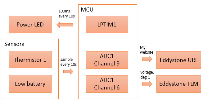
The STM32WB55 comes with an array of peripheral hardware that those familiar with the STM32 would consider to be very limited. Just one USART and an LPUART. Only four timers and two low power timers. Only one SPI. The reason for this becomes clear when you consider the requirement for low power.
These devices are expected to be battery powered and must eek out every last microwatt of energy to preserve battery life. The bottom line is that most of the time your program will be in one of the low power modes; sleeping, on standby or stopped. Hence the availability of the 'LP' peripherals that will work in some of the power-saving modes.
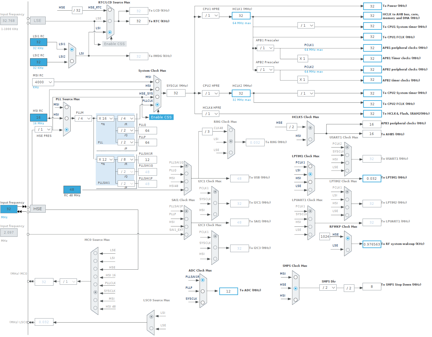
This is the clock tree that I'm going to be using. The RTC has to have an input and I'll use the LSI (more on that later). The HSE input frequency is the mandatory 32MHz which runs through the PLL to clock HCLK, ABP1 and ABP2 at 32MHz.
A branch from the output of the PLL runs through a multiplier/divider to end up clocking the ADC at 12MHz. A lower ADC clock is key to getting accurate readings. I also program the ADC to take the maximum 640.5 cycles to get a reading to get the maximum accuracy. That means that each channel will produce a reading in 53µs
There are two key software components that come with the WPAN framework: a sequencer and a hardware timer server, both of which are documented in AN5289.
Sequencer
The sequencer is a library for scheduling function calls. You provide it with a callback function pointer and an ID and then in the future you can request that the function be called with a priority that you specify. Since the sequencer main loop is called by you in your main function its callbacks will be executed in the main (non-interrupt) context.
Timer server
The timer server allows you to register a callback that should happen after an elapsed time either as a one-shot event or repeatedly at the interval you specify. The timer server works off the RTC interrupt so it's active in the low power modes.
The RTC on the STM32WB can be run off a variety of sources including the LSE at 32.768kHz, LSI at 32kHz and HSE/32 at 1MHz. I included an Epson FC135 on my board to use as the LSE but unfortunately it wouldn't start, despite using exactly the same load capacitors on a different board where it works fine.
This meant that I had to use either LSI or HSE/32 as the input source. I'd prefer to use HSE/32 because it'll be more accurate than the internal LSI but unfortunately bugs somewhere in the ST code meant that it ran way too fast and I wasn't sufficiently motivated to find the error.
I was able to get the timer server working with the LSI selected as the input to the RTC by changing the definition for CFG_TS_TICK_VAL in the USER CODE BEGIN Defines section of app_conf.h like this:
#undef CFG_TS_TICK_VAL
#define CFG_TS_TICK_VAL DIVR( (CFG_RTCCLK_DIV * 1000000), LSI_VALUE )
If this modification were not made then the timer server would be based on the 32.768kHz LSE_VALUE which is close to the 32000 LSI_VALUE but not accurate.
Application implementation
I decided to sample the battery voltage and the temperature of the first thermocouple every 10 seconds where the updated values would then be picked up by the beacon transmitter code. In app_ble.c I started a timer:
  // create a timer for sampling the temperatures at 10s intervals
  HW_TS_Create(CFG_TIM_PROC_ADC, &adcTimerId, hw_ts_Repeated, GetTemperature);
  HW_TS_Start(adcTimerId, (1000000 / CFG_TS_TICK_VAL) * 10);
Then I added the GetTemperature callback method to the same file.
static void GetTemperature() {

  // read the battery voltage [0] and the thermistor [1]

  volatile uint16_t adcReadings[2];
  ConversionComplete = FALSE;
  HAL_ADC_Start_DMA(&hadc1, (uint32_t*) adcReadings, 2);
  while (!ConversionComplete)
    ;
  HAL_ADC_Stop_DMA(&hadc1);

  // convert the battery voltage in mV

  uint32_t batteryVoltage = ((adcReadings[0] * 1800) / 4096) * 2;

  // get the voltage across the thermocouple. 10005 is the measured value of the constant
  // resistor in the divider

  float voltage = 1.8 * (float) adcReadings[1] / 4096.0;

  // calculate resistance of thermistor

  float rt = ((1.8 * 10005) / voltage) - 10005; //(voltage * resistorValue) / (1.8 - voltage);

  // convert the resistance to a temperature

  float temperature = (1 / (0.003354016 + (0.000295858 * log(rt / 10000)))) - 273.15;

  uint8_t hi = (uint8_t) temperature;
  uint8_t lo = (uint8_t) (100 * (temperature - hi) + 0.5);

  SetBeaconTemperatureAndVoltage((hi << 8) | lo, batteryVoltage);
}

void HAL_ADC_ConvCpltCallback(ADC_HandleTypeDef *hadc) {
  ConversionComplete = TRUE;
}
Sampling multiple ADC channels in one go requires interrupts and DMA on the STM32. In this implementation I start the DMA conversion for the two channels I'm interested in and then wait until I get the interrupt callback in HAL_ADC_ConvCpltCallback that sets a volatile global flag to say that the conversion is done.
Because my GetTemperature callback is registered with the timer server and not one of the regular hardware timers it will continue to operate in low power mode when many of the core peripherals are stopped.
The implementation of SetBeaconTemperatureAndVoltage is over in eddystone_tlm_service.c.
void SetBeaconTemperatureAndVoltage(uint16_t temperature, uint16_t batteryVoltage) {
  EddystoneTLM_InitStruct.BeaconTemperature = temperature;
  EddystoneTLM_InitStruct.BatteryVoltage = batteryVoltage;
}
EddystoneTLM_InitStruct is the structure that's periodically transmitted by the beacon. The Eddystone TLM implementation actually transmits a URL and a TLM at slightly different time offsets. You'll see when using a bluetooth scanner that the URL beacon usually shows up first followed slightly later by an update that adds the sensor values to it.
ST's beacon code, although quite easy to follow, appears to lag behind in the maturity of its implementation compared to the rest of the WPAN middleware. One issue is that there isn't anywhere to make user modifications that won't be overwritten if you go back to CubeMX, make a change and regenerate source code. This means that I became very adept at doing a git add ... followed by a regenerate and then a git diff to reinsert what the UI had destroyed.
Testing
Well I'm pleased to say that with relatively few iterations around the fix-test loop I had a beacon that showed up with the correct values on the Beacon Scanner android app.
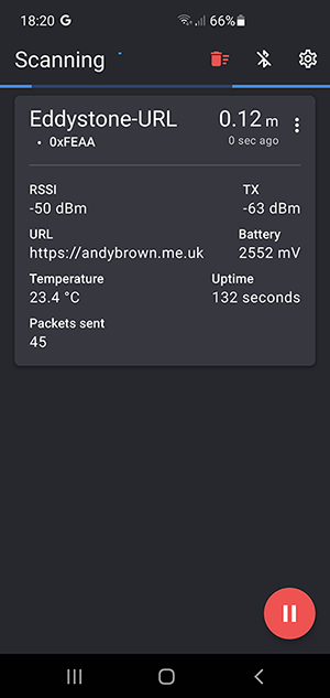
For this test the board was connected to my bench supply set to 2.5V and my room thermometer was reading 23C so I'm happy with the values sensed by the STM32 ADC.
I was pleased to see that the bluetooth range was about the same as you'd get from any commercial bluetooth device. That is, it'll go through one or two internal partition walls in a house with ease and from one floor to another if you're directly above or below it but a solid brick wall would severely dent its range.
Battery life
I set up a test to see how long a pair of rechargeable AA batteries would last. I used Duracell branded NiMH batteries with an advertised capacity of 2450mAh. They started off fully charged and I left the device transmitting continuously. Occasionally I would check in and record the date & time as well as the measured battery voltage. Here are the results:
| Date & Time | Millivolts |
|---|---|
| 06/08/2021 21:49 | 2700 |
| 07/08/2021 07:15 | 2650 |
| 07/08/2021 16:00 | 2642 |
| 07/08/2021 23:30 | 2630 |
| 08/08/2021 08:00 | 2622 |
| 08/08/2021 18:00 | 2616 |
| 09/08/2021 11:45 | 2604 |
| 09/08/2021 18:40 | 2604 |
| 10/08/2021 07:15 | 2600 |
| 10/08/2021 17:00 | 2600 |
| 11/08/2021 16:30 | 2594 |
| 12/08/2021 09:00 | 2586 |
| 13/08/2021 10:00 | 2586 |
| 13/08/2021 15:00 | 2586 |
| 14/08/2021 09:30 | 2586 |
| 15/08/2021 18:45 | 2572 |
| 16/08/2021 10:00 | 2562 |
| 16/08/2021 22:00 | 2560 |
| 17/08/2021 07:15 | 2558 |
| 18/08/2021 12:40 | 2544 |
| 18/08/2021 18:15 | 2544 |
| 19/08/2021 07:26 | 2530 |
| 20/08/2021 11:00 | 2530 |
| 21/08/2021 07:40 | 2496 |
| 23/08/2021 12:00 | 2446 |
| 24/08/2021 09:35 | 2418 |
| 24/08/2021 15:00 | 2404 |
| 24/08/2021 22:00 | 2390 |
| 25/08/2021 11:00 | 2264 |
| 25/08/2021 14:30 | 2116 |
| 25/08/2021 16:15 | 2046 |
| 25/08/2021 19:08 | 1834 |
| 25/08/2021 21:13 | 1832 |
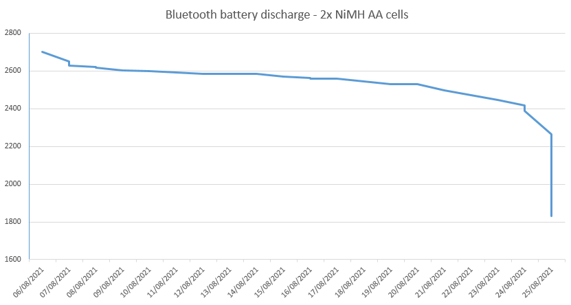
It seems that I get 20 good days of performance before the batteries tail off rapidly and the device stops transmitting. This could be improved by using non-rechargeable batteries but I find those wasteful and prefer to use the rechargeables where possible.
Future applications
Bringing all four temperature sensors to bear would be a good goal for a future firmware. I'd like to avoid having to write a custom app to do this so I might explore the Bluetooth health protocol that permits multiple thermometers to advertise their readings without having to pair and connect. The thermometers are meant to be for defined areas of the body but I don't think I'll care too much if, for example, sensor one comes up on an app as my armpit temperature!
Watch the video
If you'd like to see this board in action along with some waffling by myself then you can see the video on YouTube:
Get the source code and the Gerber files
As always, the source code to my firmware is available on Github. Click here to go direct to the repo. This project's Gerber files are also available. Click here to download. They are suitable for uploading directly to JLPCB.