Tags
Related Posts
Share This


Project Difficulty
Recent Posts
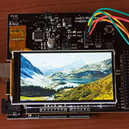
Arduino Uno R3 graphics accelerator shield uses no pins
Hello and welcome to another in my series of unique hardware projects designed to bring you something useful that you’ve hopefully never seen before and at a price point that any hobbyist can afford.
This project brings together the knowledge that I’ve gained over the last few years to bring you a graphics accelerator for the Arduino Uno R3 based on an ARM Cortex M0 core attached to a 640×360 LCD from the Sony U5 Vivaz cellphone. In previous articles you’ve seen how I’ve reverse engineered the Sony LCD and then used it in reflow oven and FPGA graphics accelerator projects.
Introduction
TFT LCD shields for the Arduino Uno are two-a-penny on ebay and the software to drive them is available from various sources but in my opinion they all suffer from the effects of trying to attach a high-frequency, high pin-count LCD to a relatively small and slow MCU.
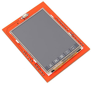
QVGA shields like this are available for as low as £3.50 delivered
- The 16MHz ATmega328 is just not fast enough to push pixels out to a high-resolution TFT at what I would call interactive speed. That is, fast enough to present a responsive user interface.
- Driving TFTs at anything like a reasonable speed needs a parallel interface, and that needs a lot of pins. You end up having hardly any left over for your actual design.
- The vast majority of these shields are 320×240 (QVGA) which looks OK up to about 2.4″ but above that the pixel density becomes too low and images appear to be low resolution, pixellated and just ‘old tech’.
- The driver code needs considerable memory resources. You can easily use up the entire 32Kb available to the Uno if you decide you want to use a couple of text fonts and forget about JPEG decoding, 2Kb is not enough SRAM.
The answer to all these problems is to offload the work of driving the LCD to a co-processor and have the Arduino communicate using a high-level command set.
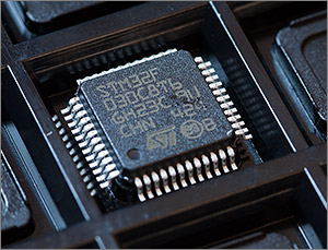
I decided to build the graphics co-processor around the STM32F0 MCU with a 48MHz core, 64Kb of flash memory and 8Kb of SRAM. It comes in a 48 pin LQFP package.
The driver software will make use of my stm32plus library surrounded by some fairly straightforward command decoding software. Multiple fonts will be supported and we’ll include JPEG decoding logic as well as compressed and uncompressed bitmap support. To assist the flash-poor Arduino we’ll include a 16Mb SPI flash IC directly connected to the ARM to provide access to fast graphics.
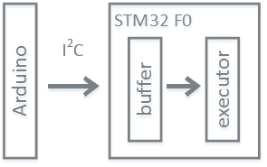
The title of this article rather cheekily states that this project will use no pins on the Arduino Uno R3. Can that really be true? Well, sort of. We’re going to communicate with the graphics accelerator over the shared I2C bus which requires use of the SCL and SDA pins but since I2C is a shared bus these pins continue to be available to other devices. That’s also why this shield is specifically for the R3 release of the Uno because it requires the two new I2C pins added on the R3.
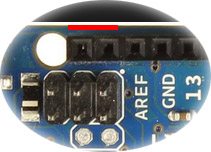
The new I2C pins below the red line
If you’ve read my previous articles you’ll know that I like to extract the maximum performance possible out of my projects and this is no exception. I’m going to optimise the Arduino library and the STM32 firmware to the absolute maximum. This should be fun, let’s get on with it.
The LCD
The LCD from the Sony Ericsson Vivaz U5 is the best all-round LCD that I have come across so far that features a built-in controller making it easy to control from a low-end MCU.
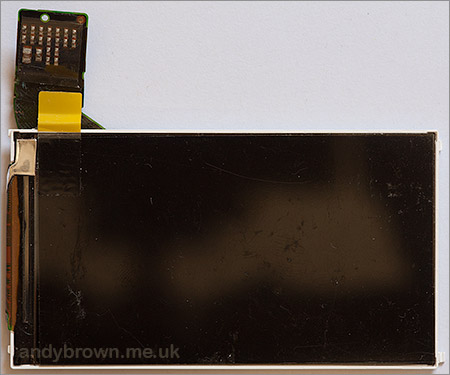
The 3.2″ display sports a resolution of 640×360 pixels which gives a density of 229ppi. This is sufficient to render graphics and text smoothly and without any of the ‘jaggies’ that make the larger QVGA screens look so poor. Another advantage is that the original displays and even many of the clones are using a wide viewing angle display technology that maintains colour fidelity even at angles approaching 180°. The only technology I know that does this is IPS but there may be others.
The display is capable of rendering up to 24-bit colour depth but because it exposes a 16-bit data bus we would need to do two transfers per pixel to support that mode. Instead, we will drive it at a 16-bit colour depth so we can transfer a whole pixel in one GPIO write. As you’ll see later in the optimisation section this will allow us to achieve an optimal pixel fill rate.
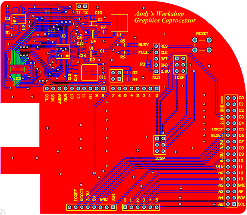
Schematic
Here’s the schematic for this design. Click to see a clearer PDF representation.
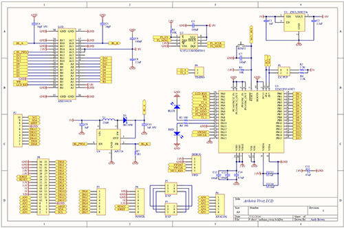
Click for a PDF
The design is very modular so let’s take a look at each section starting with the power supply.
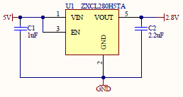
The LCD requires a 2.8V power supply and all the other components are 2.8V compatible so it makes sense for me to run the whole board at 2.8V.
The ZXCL280H5TA from Diodes Inc. is an LDO regulator capable of supplying up to 150mA which is way more than we need for the 2.8V parts of this design (the largest current consumer is the LCD backlight and that’s driven from the 5V arduino PSU).
Now let’s take a look at the big one, the MCU itself.
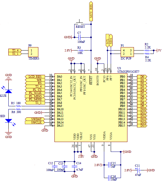
I’ve labelled the MCU as an STM32F051C8T7 which is a 64/8Kb device that I happen to have in stock. The fact is though that this project does not require the additional peripherals included with the 051 series so I recommend that you save money and use the STM32F030C8T6 currently available for £1.23 from Farnell.
Port B is given over entirely to the 16-bit LCD data bus so we can write out a full 16-bit pixel in one operation. Driving the LCD at 16 bits per-pixel gives us a maximum of 64K colours. The remaining control signals (LCD_RES, WR and RS) are mapped to PA0..2.
The SPI flash IC is connected to PA4..7 which corresponds to the SPI1 STM32 peripheral so we can use hardware support to drive the SPI flash at the maximum speed permitted by the STM32.
The I2C interface is connected to PF6..7 which corresponds to the I2C2 STM32 peripheral so again, we can use hardware support for the I2C protocol. This device will be an I2C slave which means that the Arduino will be driving the I2C clock and data lines at 5V TTL levels. PF6 and PF7 are marked as “FT” in the datasheet which means that they are 5V tolerant and will not burn out when they receive 5V levels.
P1 is a jumper block that connects the I2C bus pullup resistors. I2C requires one pair of pullups per bus so this jumper block allows the pullups to be disconnected if some other device on the bus is providing the pullups.
A physical reset button is provided so that I can easily reset the board if it happens to get out of sync with the Arduino (it happens if restarts are accidentally staggered).
I will use the blue LED on PA9 to indicate activity as commands are received and processed. The red LED on PA10 will be a ‘buffer full’ indicator that will come on if the Arduino manages to fill up the STM32’s command buffer, causing the I2C bus to stall until space is available. The operating voltage of 2.8V does limit the choice of LED colours that I can use with this simple circuit but blue and red will be fine.
Not wanting to waste any STM32 pins, I decided to expose PA3 and PA8 as pin headers that the Arduino can drive either as GPIO or timer output pins. The STM32 has powerful timer functionality that can be used to generate PWM and other timer-based waveforms with no CPU overhead.
The two-wire SWD debug interface is broken out to a pin header so that the STM32 can be programmed in-circuit using the cost-effective ST-Link/v2 debugger.
Decoupling is provided according to ST’s recommendations and a bulk 47-100µF electrolytic is provided to provide low frequency decoupling for the whole board.
Let’s move on to the LCD connector.
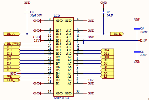
The AXE534124 is a 34 pin 0.4mm connector made by Panasonic and sold only by Digikey in the US, this makes it quite expensive for non-US citizens to get hold of but nevertheless Digikey will ship it to us but we have to deal with the customs fees.
The socket has quite short legs and is a bit of a pain to solder. I do it by reflow to get it tacked down and then use lots of flux and a very fine tip iron to touch up any loose legs under the microscope.
I discovered the pinout for this LCD during my reverse engineering article and the additional decoupling capacitors are the same as you can find in Sony’s official schematic for the cellphone.
The backlight for this cellphone consists of 6 white LEDs in series. We have no information as to the forward voltage of this LED string so we’ll drive it using a constant current LED driver.
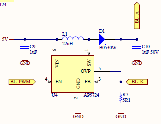
The AP5724 from Diodes, Inc. is a boost converter that works by raising its output voltage until a preset current flows through the LED string.
The 5.1Ω resistor, R7 sets the constant current to 20mA. The backlight intensity is varied by applying a PWM signal to the EN pin and the Renesas R61523 controller in the LCD panel is slightly unusual in that it can generate that PWM signal itself, which saves us an MCU pin.
I think we’re done with the LCD-related circuitry, let’s move on to the flash memory.
Spansion S25 flash devices come in SOIC-8 packages that are either 150 or 208mil wide. I got my first batch of boards printed to accept the 150mil footprint and have fitted them out with the 16Mb S25FL216K device.
The 208mil width is perhaps the more common format as capacities increase beyond 16Mb so if you opt to download the Gerbers for this project then you’ll find that the flash footprint is for the 208mil device. You can choose just about any of the S25 range but make sure you select the 208mil width.
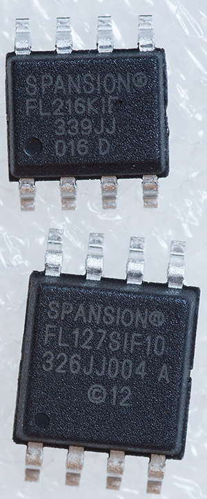
The IC at the top is a 16Mb flash IC in 150mil format and the one at the bottom is a 128Mb device in 208mil format.
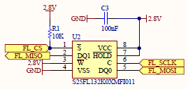
The interface to the flash IC is plain SPI and we map that directly to the SPI peripheral on the STM32 MCU. Even the lowly STM32F0 has a DMA peripheral that permits us to operate the flash memory asynchronously to the MCU core and at the MCU’s full permissable clock speed.
The remainder of the schematic concerns the pin headers. There’s lots of them. Most are devoted to connecting down into the Arduino sockets so that we can break out all the pins to a separate header where you can access them for GPIO.
Bill of materials
Here’s the full bill of materials for this project.
| Designator | Value | Description | Footprint | Comment |
|---|---|---|---|---|
| BLUE | Blue LED | 0603 | ||
| RED | Red LED | 0603 | ||
| C1, C9, C15 | 1µF | Ceramic cap | 0603 | |
| C2, C8 | 2.2µF | Ceramic cap | 0603 | |
| C3, C6, C7, C12, C13 | 100nF | Ceramic cap | 0603 | |
| C4, C5 | 56pF 50V | Ceramic cap | 0603 | |
| C10 | 1µF 50V | Ceramic cap | 0805 | |
| C11 | 100µF | Panasonic FC-D electrolytic | Case D | approx 47-100µF |
| C14 | 4.7µF | Ceramic cap | 0805 | |
| C16 | 10nF | Ceramic cap | 0603 | |
| D1 | B0530W | Schottky diode | SOD123 | Any compatible SOD123 schottky |
| DEBUG | HDR1X5 | Header, 5-Pin | 2.54mm male | |
| L1 | 22µH | CDRH5D28 | 6x6mm | |
| LCD | AXE534124 | 34 pin connector | 17×2 0.4mm | |
| P1 | HDR2X2 | Header, 2-Pin, Dual row | 2.54mm male | |
| P2 | HDR1X10 | Header, 10-Pin | 2.54mm male | |
| P3, P4 | HDR1X8 | Header, 8-Pin | 2.54mm male | |
| P5 | HDR2X3 | Header, 3-Pin, Dual row | 2.54mm male | ICSP (front) |
| P7 | HDR2X3 | Header, 3-Pin, Dual row | 2.54mm female | ICSP (back) |
| P6 | HDR1X6 | Header, 6-Pin | 2.54mm male | |
| P8 | HDR2X18 | Header, 18-Pin, Dual row | 2.54mm male | |
| P9 | HDR1X2 | Header, 2-Pin | 2.54mm male | |
| R1, R3 | 10KΩ | Resistor | 0805 | |
| R2, R4 | 2.2KΩ | Resistor | 0805 | |
| R5 | 180Ω | Resistor | 0805 | |
| R6 | 390Ω | Resistor | 0805 | |
| R7 | 5.1Ω | Resistor | 0805 | |
| RESET | make type | PCB button | through hole | |
| U1 | ZXCL280H5TA | 2.8V regulator | SOT353-5N | |
| U2 | S25FL132K0XMFI011 | 32Mb flash | SOIC8 (208) | Others are possible |
| U3 | STM32F051C8T7 | STM32 Cortex M0 | LQFP48 | STM32F030C8T6 is compatible |
| U4 | AP5724 | LED driver | SOT26 |
The reset button is the 6x6mm button that you can easily find on ebay if you search ‘pcb button’. It’s the one with the silver top, black button and four little black corner posts.
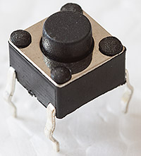
These buttons do come in different sizes so make sure you get the 6x6mm variant.
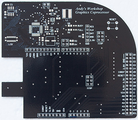
PCB layout
The PCB layout is all based around the restrictions of having to fit onto the Arduino Uno as a shield.
The attached 80x45mm LCD dominates the surface of the PCB between the rows of Arduino pin headers so the control circuitry is located offset to the top of the PCB where it overhangs the edge of the Arduino. The assumption is that this will be at the top of any shield stack that you have because if it wasn’t then you wouldn’t be able to see the LCD.
There are cutouts placed in the PCB where the Arduino’s power supply and USB connector are located because these parts protrude upwards just enough to interfere with the PCB. I didn’t need all of the space on the top so instead of cutting it off sharp I designed it with a curved edge. There’s no design need for this, it just looks nice.
Printing the boards
The design fits within a 10x10cm square so I was able to use the low-cost printing service at Elecrow to get the design printed.
LCDs look best against a black background with the idea being that there’s nothing standing out that distracts your eye from the image displayed on the screen and for that reason I reluctantly went for the gloss black solder mask. I say ‘reluctantly’ because the black soldermask is probably the hardest to work with. The contrast is low so traces are difficult to see, flux stains are easily visible and the white silkscreen discolours to light brown easily under reflow. If, like me, you own a black car then you’ll know what it’s like trying to keep it clean. Cleaning black PCBs is just as difficult!
Assembling the board
This isn’t a difficult board to assemble. It’s fairly low density and the parts are of a manageable size for SMD. I reflowed all the SMD parts using my reflow oven and then soldered all the through-hole components and pin headers manually.
Click for larger
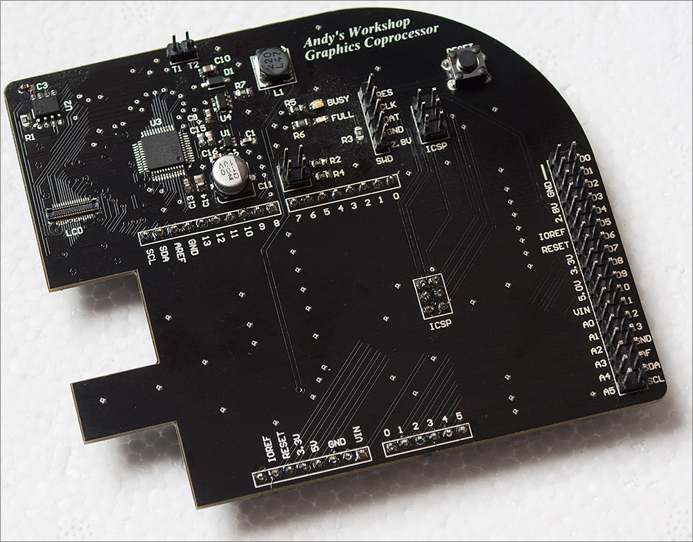
The front side shows all the components, upward facing pin headers and the space for the LCD panel. The panel will be mounted on double-sided sticky pads to lift it clear of the PCB.
Click for larger
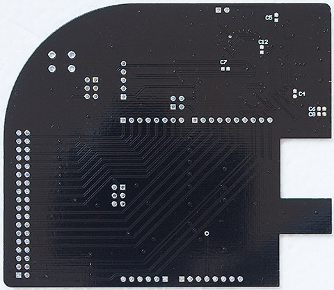
The rear side shows the few capacitors mounted on the rear and the downward facing pin headers. Note the 2×3 ICSP female header that mates with the male header on the Arduino board so that it can be relocated on the top of this board.
Click for larger
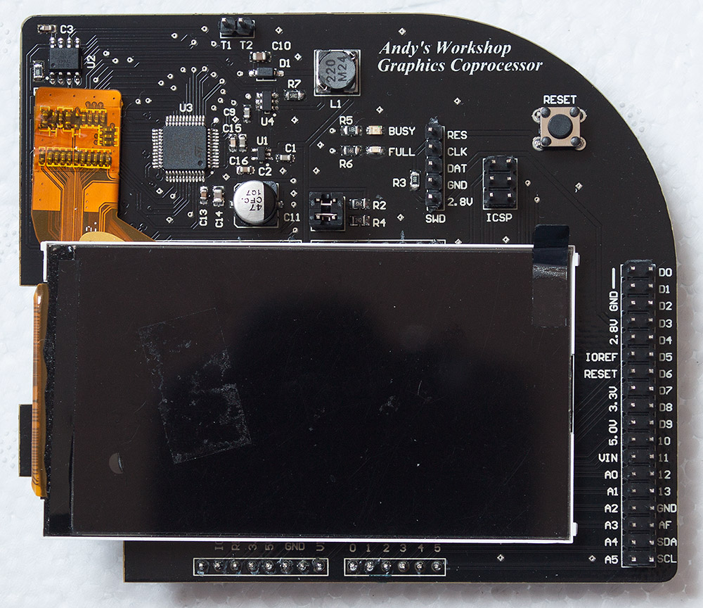
The picture above shows how it looks with the LCD fitted to the board. The plug on the FPC tail presses into the corresponding receptable on the board leaving the panel sitting between the two rows of Arduino pins. The LCD is mounted on double-sided sticky pads to lift it clear of the traces and vias on the back of the PCB.
The STM32 firmware
The basic idea behind the graphics accelerator is a master-slave arrangement whereby the Arduino is the I2C master and the STM32 is the slave. High-level commands such as ‘draw line from a to b’ or ‘draw text at point p’ will be sent from the Arduino and queued for execution in a circular buffer by the STM32. If the buffer should fill up then the STM32 will suspend the I2C bus until space becomes available.
The I2C management code will be IRQ-driven and the graphics operations will run in the normal CPU context. The graphics operations will reflect those available in my stm32plus library:
- Backlight brightness operations
- Sleep, wake, gamma set operations
- Set foreground, background colours
- Draw rectangle, fill rectangle
- Clear screen
- Gradient fill rectangle
- Draw line, draw polyline
- Plot individual points
- Draw ellipse, fill ellipse
- Raw panel operations (set window, write raw data)
- Select font, draw text, draw text with filled background
- Draw bitmap from arduino or onboard flash with optional LZG compression
- Draw jpeg from arduino or onboard flash
- Erase and program the onboard flash
- T1, T2 pin GPIO and/or timer/PWM options
When you instantiate an stm32plus LCD driver you do so by supplying the orientation, colour depth and driving mode as compile-time template constants. This allows the compiler to produce optimal code for your use case without wasting cycles executing conditions like ‘if portrait then … else …’ when such conditions will always only go one way. It also means that I’ll need to provide firmware that runs the LCD in portrait and landscape mode.
This LCD has a natural 16:9 widescreen aspect so all my examples will be designed to run in the 16:9 landscape orientation.
The core loop of the firmware that you can see in CommandExecutor.cpp looks like this:
  for(;;) {

    // wait for data to become available

    while(_commandBuffer.availableToRead()==0) {

#if !defined(DEBUG)
      // go to immediate sleep mode. will wake immediately on data arrival (IRQ)

      __WFI();
#endif
    }

    // keep the busy light on while buffered commands are processed

    _indicators.setBusy(true);

    do {
      processNextCommand();
    } while(_commandBuffer.availableToRead()!=0);

    // buffered commands processed, switch off the indicator

    _indicators.setBusy(false);
  }
The STM32 core stays in sleep mode until woken up by the I2C IRQ that indicates data has arrived from the Arduino. The IRQ handler deposits the data in the circular buffer and returns, which means that the next time this loop calls availableToRead() it will return a non-zero value.
The wake-up from sleep operation is immediate and has zero cost in terms of cycles. It’s ifdef’d out for debugging because the debugger gets really confused when it can’t communicate with an asleep MCU.
The interrupt handler that receives and deposits data into the SRAM circular buffer looks like this. You can see the full source code in CommandReader.h.
void CommandReader::onInterrupt(I2CEventType eventType) {

  bool full;

  switch(eventType) {

    case I2CEventType::EVENT_ADDRESS_MATCH:
      _addressReceived=true;
      break;

    case I2CEventType::EVENT_RECEIVE:                 // data received

      // got some data

      _addressReceived=false;

      // write the byte

      _commandBuffer.write(I2C_ReceiveData(*_i2c));   // add to the circular buffer

      full=_commandBuffer.availableToWrite()==0;
      _indicators.setFull(full);                      // set/reset the full LED

      // is the buffer full? Suspend incoming if it is.

      if(full)
        _commandBuffer.suspend();

      break;

    case I2CEventType::EVENT_STOP_BIT_RECEIVED:
      if(_addressReceived)                            // no data in frame? must be a reset request
        NVIC_SystemReset();
      else
        _addressReceived=false;
      break;

    default:
      break;
  }
}
The suspend() operation simply masks off all interrupts at the NVIC level, this has the effect of halting I2C communication until we unmask interrupts again.
The circular buffer implementation, which you can see here, is designed to be safe in the common scenario of an IRQ writer and a normal code reader.
There’s some additional logic in there to detect when a zero length packet is received, and if it is then the MCU gets reset. This is my way of remotely resetting the STM32 from the Arduino that should work even in cases where the main MCU core has hung but the I2C bus is still operational.
Click for larger
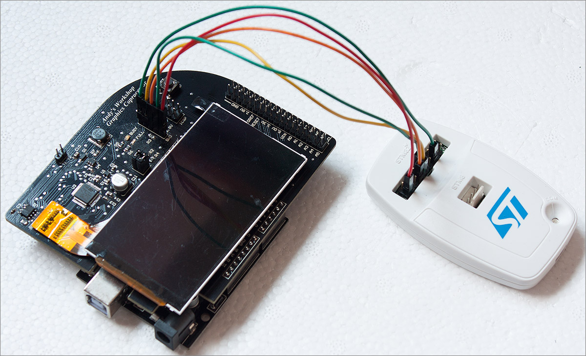
The photograph shows the board, with LCD connected and wired up to the ST-Link/v2 debugging and programming dongle. If you’re not interested in modifying the firmware then you can just use ST’s official application and driver to upload the hex file included with the firmware on github.
Testing
To test the board I created a suite of Arduino sketches that exercised the capabilities of the graphics library. The STM32 was hooked up to the ST-Link/v2 debugger so that I could perform single-step debugging in the Eclipse GUI.
Click for larger
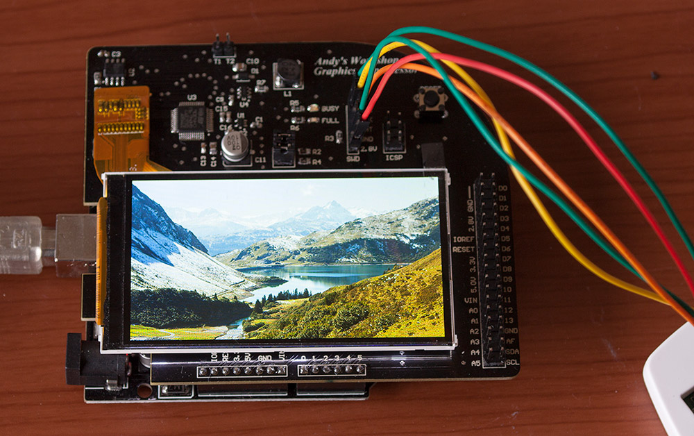
The photograph shows the board displaying a JPEG image that was stored on the onboard flash IC and then decoded and displayed by the STM32.
Optimisation
Now that I’ve got a stable baseline I can turn my attention to the fun topic of optimisation. The system is already very fast and meets my goals, but can I make it faster?
Optimising the Arduino library
The Arduino library is very simple, and it needs to be with so few resources available in the little ATmega32 yet any gains made here could have the biggest impact. Let’s see how we can structure our C++ code to give the compiler the best chance to produce the smallest output.
Back in the old days C++ programmers were tought to place their class definitions in header files and the implementations in source (cpp) files. It made for a clear distinction between design and implementation but unfortunately it results in suboptimal code generation when we use a modern C++ compiler.
When the compiler needs to make a call to, for example, int foo(int a,int b) it consults the information it has about that function, or class method, and in the case where it can only see a signature declaration it must fall back to the default calling strategy. Registers will be stacked, parameters will be registered and/or stacked and a branch will be made. Afterwards the return value will be registered and the saved registers unstacked. This is all costly both in time and space but because all you’ve given the optimiser to work with is a method signature then that’s all it can do for you. Tough luck.
Fortunately we can improve on that by using the most misunderstood and worst-chosen keyword name in the C and C++ language: inline. I still today see people who should know better claim that it directs the compiler to place a function definition inline to the calling code which thereby makes your code bigger. It absolutely does not do that, despite the misleading name.
The effect of the inline keyword is to suspend the usual behaviour of the one definition rule and allow a definition to appear in multiple translation units (source files) as long as they are all identical. Incidentally, gcc cleverly achieves this by marking inline functions as weak references. In a modern compiler the inline keyword is little more than a linkage modifier.
When you declare everything inline you are giving the optimiser all the information it needs to do a complete job on your source file to achieve the goals that you have told it achieve with the optimisation flags that you gave on the command line. Most gcc users will select one of the -O options that are shortcuts for large collections of individual -f options.
Since the Arduino IDE is preset to compile with the -Os option, the optimiser will not do anything to increase code size. So if it would increase code size to place a method inline, it won’t do it. If a method is very small and consists of fewer instructions than the lengthy standard call procedure, it will be placed inline where it will be optimised as an integral part of your method. It will do this to any function where it can see the whole body, regardless of whether or not you declare it to be inline.
To see the effect of this I created my library once as an old-style cpp/h combo and then again as all inline. I used the GraphicsMethods example to test it because it makes a lot of library calls. The net result was that the compiled binary was about 500 bytes smaller when everything was declared inline. On these small MCUs differences such as that can be very significant. I suspect I could make further significant gains by optimising the poorly implemented Wire Arduino library class but for now this will do.
Are there any disadvantages? Not many. You’ll still need .cpp files around to instantiate any static class data members and ISR implementations that you’ve got – static functions at namespace level can stay inline and go to internal namespaces to keep them from causing trouble. Working around circular dependencies can be trickier but it’s always possible to overcome those by improving your design.
Optimising the STM32 library
I’ve already spent some time optimising the stm32plus library driver as far as it’s feasible to go. The entire access mode is hand-written in assembly language to squeeze the last bit of performance possible out of the core pixel transfer code. I wrote about that development here in the LG KF700 reverse engineering article. The full assembly language source code to the access mode optimised for the 48Mhz F0 is here on github.
Let’s see what optimisation I can achieve with my STM32 firmware.
Firstly I decided to tune the optimisation options that I was using on a per-file basis. I needed to use the -Os option on the bulk of the source files just so I could squeeze it all in to the 64Kb flash memory on the F0 but I had enough room to enable the -O3 high performance option on the CommandExecutor class that handles the core loop of retrieving commands from the circular buffer and handing them off for execution. With these optimisations my build stats are:
   text    data     bss     dec     hex filename
  59872     112    1244   61228    ef2c build/release/awcopper.elf
With the firmware fully optimised it’s time to take a look at how it’s performing. Let’s break out the logic analyser and probe the pixel write-cycle to see how it compares with the fastest permitted by the R61523 datasheet, and if it falls short then I’ll examine the options available to me to make it as close to optimal as I can get.

Click for larger
The screen grab from my logic analyser shows that the combined write cycle is taking 83ns and this is the code that does it, taken from the access mode class:
str  %[wr], [%[creset], #0]  // [wr] = 0
str  %[wr], [%[cset], #0]    // [wr] = 1
The Cortex-M0 takes 2 cycles to execute a str instruction (and on the M0 it actually does take 2 cycles unlike the F4 which uses its instruction pipeline to mess up your carefully calculated cycle counts). Running at 48Mhz, each cycle is 1/48000000 = 20.83ns so our measured result of 83ns equals the expected result of 4×20.8 = 83.3ns.
Let’s see how the 83ns write cycle compares to the limits imposed by the R61523 controller.
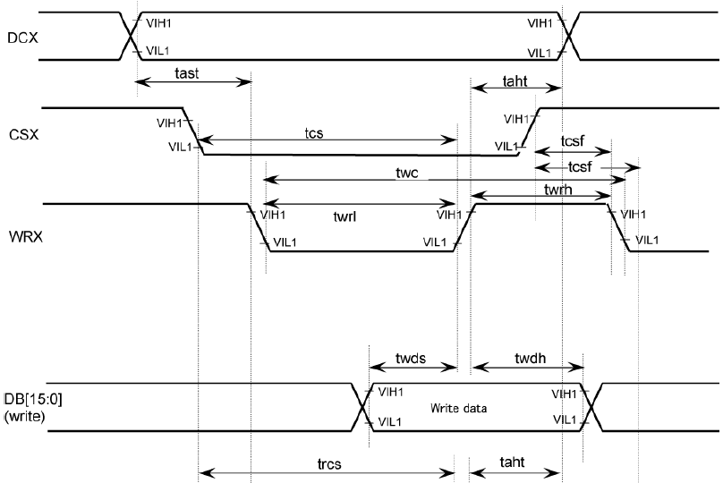
Click for larger
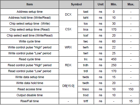
In the above image the important timings for us are twds (data setup), twdh (data hold) and twc (write cycle). The timings related to the CS (chip select) signal are irrelevant because we keep it tied to ground. Here’s the table of limiting values.
The controller clocks in the data on the rising edge of WR. The data setup time (twds, min 15ns) is the minimum time that the data must be present before the WR control line goes high. We set up the data before we pull WR low so our data setup time is at least 2 clock cycles which is well within the limits.
The data hold time (twdh, min 20ns) is the time that the data must remain present after WR has gone high. Again for us that is at least 2 clock cycles so we are well within the spec again.
Now lets looks at the overall write cycle time limit. It’s 60ns and we’re clocking it at 83ns. The controller can go faster but seemingly we’re stuck because our code cannot be written any more efficiently. Or are we…
Let’s overclock the STM32.
Overclocking the STM32
Overclocking is something that’s come to be associated with PC hardware enthusiasts seeking to squeeze the last bit of performance out of their CPUs, memory and graphics cards by tweaking the values of system clocks and voltage levels at the expense of heat generation and sometimes overall system stability. But can we overclock an MCU and what does it mean if we do?
The simple answer is that it’s trivially easy to raise the core clock of the M0 from 48MHz to 64MHz. Every F0 application that runs at a clock speed higher than its reference oscillator is going to have some startup code that sets the value of the system clock from a PLL whose frequency is calculated from the reference oscillator and some multipliers and dividers.
For example, this board runs the F0 from its internal oscillator using the PLL to generate a 48MHz clock like this:
  /* PLL configuration = (HSI/2) * 12 = ~48 MHz */
  RCC->CFGR &= (uint32_t)((uint32_t)~(RCC_CFGR_PLLSRC | RCC_CFGR_PLLXTPRE | RCC_CFGR_PLLMULL));

  RCC->CFGR |= (uint32_t)(RCC_CFGR_PLLSRC_HSI_Div2 | RCC_CFGR_PLLXTPRE_PREDIV1 | RCC_CFGR_PLLMULL12);
  /* Enable PLL */
  RCC->CR |= RCC_CR_PLLON;
Note the RCC_CFGR_PLLMULL12 PLL multiplier of 12 which calculates 8MHz / 2 * 12 = 48MHz. The maximum value that this multiplier can take is 16. So to overclock the F0 to 64MHz it really is as simple as this:
  /* PLL configuration = (HSI/2) * 16 = ~64 MHz */
  RCC->CFGR &= (uint32_t)((uint32_t)~(RCC_CFGR_PLLSRC | RCC_CFGR_PLLXTPRE | RCC_CFGR_PLLMULL));

  RCC->CFGR |= (uint32_t)(RCC_CFGR_PLLSRC_HSI_Div2 | RCC_CFGR_PLLXTPRE_PREDIV1 | RCC_CFGR_PLLMULL16);
  /* Enable PLL */
  RCC->CR |= RCC_CR_PLLON;
The core clock will now run at 64MHz, a healthy 33% increase over ST’s stated limit. However, there are other issues that we need to be sure we’re happy with. Any internal clock that is sourced from the system clock is going to be ticking faster than expected and that includes the peripheral clocks.
The good news is that my overclocked F051 boots up and runs just as stable and without any noticeable increase in temperature over the 48MHz version. Now let’s take a look at our LCD write cycle times:
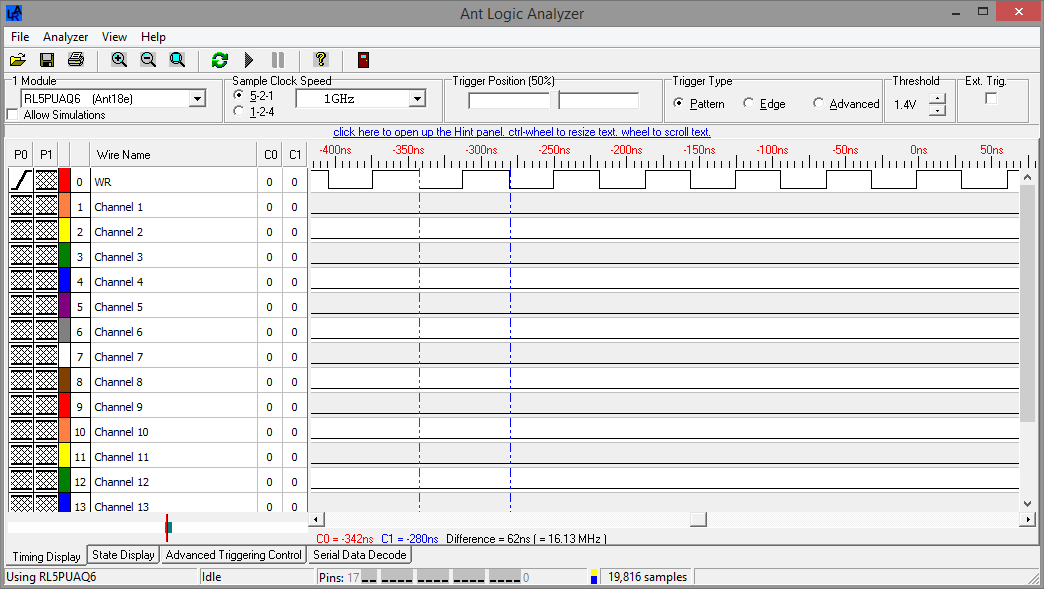
Click for larger
The write cycle is now 62ns which is right where we would calculate it to be given the new MCU cycle time of 15.625ns. That’s more like it, we’re only 2ns off the stated minimum write cycle and with the setup and hold times still within spec that’s about as close to the limit as I want to go.
There’s still the peripheral clocks to deal with. They’re going to be ticking at higher rates and we need to make sure that they are still working OK.
The SysTick clock is a core part of every Cortex-M0 and we use it internally to perform accurate millisecond delays. The stm32plus MillisecondTimer class initialises SysTick using ST’s standard peripheral library call:
SysTick_Config(SystemCoreClock / 1000);
The SystemCoreClock variable is a uint32_t set by ST in the startup code to the value of the core clock in MHz. We simply change it from 48000000 to 64000000 and SysTick is back to ticking at 1ms.
The I2C bus is next for consideration. In this board we’re using it as a slave, the clock is generated by the Arduino therefore there is nothing to do here. Our bus continues to operate at the frequency selected by the Arduino library.
Finally, the SPI bus needs to be checked out. The SPI clock is generated from the core clock and a divider. The minimum value of the divider, which is the value we are using, is 2, giving a SPI clock of 24MHz. Let’s verify that with the logic analyser.
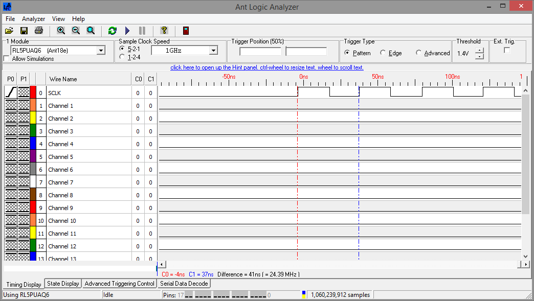
Click for larger
It’s as expected, the clock is operating at around 24MHz. Let’s see how it looks after the overclocking. The SPI flash IC has a limit of 44MHz that we cannot exceed.

Click for larger
The clock frequency is up 30% to 31.25MHz which is within the limits of the flash IC and represents a nice speed increase for this project.
We’re not using any other peripherals so the effect of the overclocking on those peripherals is not investigated here.
Video introduction
I made up a little video in which I talk through the build process and give a brief tour of the board. You can watch it on the embedded player here but you’ll get better quality if you click here to go to the YouTube site and watch it there.
Firmware resources
If you’re considering building one of these boards yourself, and I do encourage you to try because it’s not difficult, then here’s a list of the resources you’ll need to complete the firmware side of the project.
The STM32 firmware
You can download a release from github or you can check out the master branch. If you don’t want to compile the firmware yourself then you can just flash one of the pre-built .hex files using the ST-Link/v2 utility.
Building the firmware yourself will require that you have first built and installed stm32plus. Assuming you’ve done that you can then use scons to build the firmware. There are several build options:
$ scons
scons: Reading SConscript files ...

Usage: scons mode=<MODE> [-jX | -c] [overclock=yes]

  <MODE>: debug/release.
    debug   = -Og
    release = combination of -Os and -O3

  [overclock]
    specify this option to overclock the MCU to 64MHz

  Examples using -j to do a 4-job parallel build:
    scons mode=debug -j4
    scons mode=release overclock=yes -j4

  The -c (clean) option removes the build output files.
The build options allow you to build the debug or release version with or without overclocking support. Note that a debug build only has a single font available due to the increased size of the compiled binary. The full complement of 9 fonts is included with the release build.
The Arduino library and examples
The Arduino library and examples are an integral part of the source code on github. To install, simply extract the contents of awcopper.zip into your Arduino ‘libraries’ directory. I have tested the library on version 1.0.6 of the Arduino IDE.
The Arduino examples
Each one of the Arduino examples demonstrates a different capability of the firmware. Here’s a brief overview of each one.
GraphicsMethods
This one demonstrates all of the graphics primitives, excluding those that operate on the SPI flash IC. Since the graphics commands are streamed across the I2C bus to the STM32 it makes perfect sense to use the C++ << operator to stream commands to the graphics library. For example:
  copro << awc::foreground(awc::WHITE)        // set foreground to white
        << awc::font(awc::ATARI)              // select the Atari font
        << awc::text(Point::Origin,"hello");  // text string at the origin
Here’s a video that shows the GraphicsMethods demonstration in action. It’s a bit small embedded here in the page so click here to open it up on the main YouTube site where the quality will be better.
ProgramFlash
This demonstrates how to program bitmaps into the flash IC using your PC to send the bitmaps over the USB cable to the Arduino. A small PC application UploadToFlash.exe, written in C#, is provided in the utilities directory of awcopper.zip that handles the PC side of the operation.
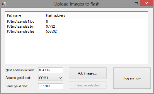
To use, first compile and flash the Arduino example. It will erase the flash IC and then sit there waiting for data to arrive from the PC.
Now run UploadToFlash.exe and use it to select the bitmaps to upload to the flash IC. You can specify the page address in bytes of each one to upload. The address will be automatically increased by the size of each image you add. You can add jpegs, uncompressed images and LZG compressed images.
Note that the address of each image must be aligned to a 256-byte page in the flash IC.
Uncompressed and LZG images can be created from JPEGs, PNGs etc. by the bm2rgbi.exe C# utility included with stm32plus and also included here in the utilities directory of awcopper.zip. It’s a command line program, here’s an example of how to create an uncompressed image from a JPEG.
$ bm2rgbi.exe sample2.jpg sample2.bin r61523 64
Width:  640
Height: 360
Format: Format24bppRgb
Writing converted bitmap
Completed OK
Here’s another example that shows how to create an LZG compressed image from a JPEG. LZG is very similar to PNG in its operation but is optimised for use on a small MCU.
$ bm2rgbi.exe sample2.jpg sample2.lzg r61523 64 -c
Width:  640
Height: 360
Format: Format24bppRgb
Writing converted bitmap
Compressing converted bitmap
Compression completed: 460800 down to 213021 (53%) bytes
Completed OK
When you’ve got all your images lined up in the PC application and your Arduino is ready and waiting then just click Program Now and wait for it to finish.

Click for larger
The picture shows the flash programmer after its finished programming. Each green square represents a page that’s been programmed and verified.
FlashBitmaps
This example shows how to display images stored in the flash IC. JPEGs, uncompressed and LZG (see above) images are all supported. The example program will show one of each to give you an idea of the difference in execution speed.
Uncompressed bitmaps are limited mostly by the speed of the SPI bus whereas LZG and JPEG images spend a significant portion of their time being decompressed by the STM32. The code that I wrote to interact with the flash IC uses DMA transfers from the SPI bus to make optimum use of the bus frequency and to allow us to interleave image processing with the data transfer from the SPI bus.
The code used to display a JPEG image is very straightforward:
const Rectangle fullScreen(0,0,Copper::WIDTH,Copper::HEIGHT);
copro << awc::jpegFlash(fullScreen,JPEG_SIZE,JPEG_ADDRESS);
Like all other commands, this will be streamed across as a minimal number of bytes to the STM32 where it will be executed asynchrously, freeing up your Arduino to immediately do other things while the image is being obtained from flash and rendered on screen.
Here’s a video that shows the process of programming the onboard flash and subsequently running a demo that shows the different types of bitmaps being displayed. Click here to view it in high quality on the YouTube website.
GpioPins
This example demonstrates how to program the T1 and T2 pins as GPIO outputs from the STM32. The example will toggle them on and off at 1Hz while displaying an alternating image on the screen.
You could hook up these pins to a pair of LEDs to see them in action. Remember that the STM32 is operating at 2.8V so the output high level on the pins is 2.8V. Please take care not to source or sink current in excess of the limits documented by the STM32 datasheet or damage may occur.
TimerPwmPin
This example shows how to program the T1 and T2 pins using the STM32 timer peripheral to generate alternating PWM waveforms. On the STM32 timer waveform generation is handled in hardware and has no impact on the operation of the MCU core.
The example will vary the duty cycle of the PWM waveform up and down from zero to 100% while showing a graphical preview of what it will look like. Here’s a video that shows the example in action. I’ve wired T1 and T2 to LEDs so you can see the actual output.
Build your own PCB
If you’d like to build this project yourself then you’ll need a PCB and the parts listed in the bill of materials section as well as a Vivaz U5 LCD that you can get on ebay. You can get the gerbers for the PCB from my downloads page.
The PCBs can be ordered from ITead, Elecrow or Seeed Studio in batches of 10. You’ll need to order the 10x10cm option. I generally use Elecrow but they’re all the same quality so if you have a personal favourite then go ahead and use them.
You don’t have to use black, and you’ll save yourself some cursing if you don’t. Green and red both reflow and clean up very well. Blue less so, but still OK. Yellow looks OK to me but may be a bit of an acquired taste and I don’t think it would contrast well with the LCD. White is like black, but worse. Traces are invisible and flux stains shout out ‘look at me!’. Avoid white. I wrote an article about selecting solder mask colours, have a read if you’re unsure.
Future improvements
There’s always room for improvement and I’ve had a few ideas that could be implemented in a ‘version 2’ of this project.
- Synchronised resets. The STM32 board should be slaved to the Arduino’s reset line. Currently you have to ensure that the two boards are reset quite close together to avoid the risk of the I2C stream coming from the Arduino being misinterpreted by the STM32. This could be achieved with a reistor divider to ensure that the 5V Arduino reset level is translated to 2.8V.
- TE support. The TE (tearing effect) LCD output signal could be used to synchronise writes to the LCD so that graphics could be drawn flicker-free.