Tags
Related Posts
Share This


Project Difficulty
Recent Posts
Modding the STM32 F4 Discovery with a 25MHz clock
In this article I’m going to show you how to do a straightforward modification to the STM32 F4 Discovery board that will change the onboard oscillator from 8MHz to 25MHz.
Why do this
Probably the main reason to do this is ethernet. If you’re prototyping an MII ethernet PHY then that PHY will need a 25MHz reference clock. All those that I’ve seen do allow you to supply such a clock directly from a crystal connected to the PHY but why have two 25MHz crystals on your board if you only need one? The STM32 F4 has an MCO (Main Clock Out) pin that is intended to drive the 25MHz clock on an ethernet PHY.
However ethernet is not the reason why I’m doing it. As the maintainer of the stm32plus STM32 C++ library I need to keep a set of reference boards around for testing. I’ve got F1 boards with 8 and 25MHz oscillators but I only have 8MHz F4 boards. The cheapest and easiest way for me to get a board with a 25MHz reference clock is to take a discovery board and mod it with an off-the-shelf 25MHz crystal. Hence this article.
Planning the modification
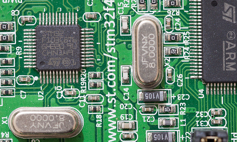
The first step in the planning of this operation is to get hold of the schematic for the F4 discovery board. That’s easy, ST publish it in the back of their user guide. Here’s the section that contains the external oscillator.
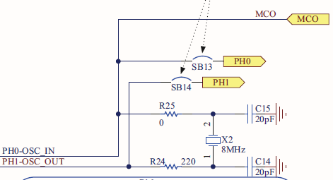
All crystal ‘can style’ oscillators require a pair of external loading capacitors whose value can be calculated from the load capacitance value published by the crystal manufacturer. ST don’t tell us the load capacitance for the crystal that they’ve selected but that’s OK because I don’t need to know. All I need to know is that the capacitors in-situ are 20pF each.
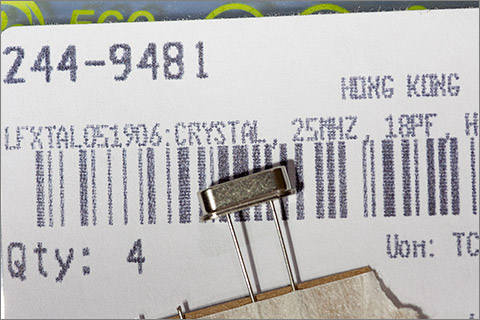
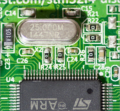
I will be replacing the 8MHz ‘X2’ crystal with a 25MHz replacement that I got from Farnell. It requires 18pF of load capacitance.
The formula for choosing the values of the two load capacitors is well documented on the internet. It is:
C1 = C2 = 2 * CL - (CP + CI)
Where CP is the parasitic capacitance of the board and CI is the input capacitance of the MCU. For my crystal with its CL of 18pF this works out at C1 = C2 = 30pF, assuming the commonly quoted CP + CI = 6pF.
The ST load capacitors are 20pF each so I will need to replace those with a pair of 30pF ceramic capacitors in 0603 format. No problem.
ST’s 8MHz crystal (X2) has a 220Ω resistor in series with it, labelled R24 on the schematic. My replacement crystal does not require any additional series resistance so I will be replacing R24 with a 0Ω bridging resistor.
In addition to the component substitution I will need to make some modifications to tell the discovery board to actually use X2.
The STM32F407 can take its clock source either from an internal 16MHz oscillator, known as the high speed internal (HSI), or an external clock source such as X2 on the discovery board, known as the high speed external (HSE). With its 1% frequency tolerance, HSI is not particularly accurate and that’s one of the reasons to use the HSE.
With X2 populated by an 8MHz crystal on the discovery board it might look like that’s where the clock is being sourced from but in the default form that’s not the case. That 8MHz clock is actually coming from the master clock out (MCO) pin of the STM32F103 that’s providing the ST-Link interface. If we want the STM32F407 to get its clock from X2 then we must remove a resistor, R68.
So, to summarise the actions I’ll be taking:
- Remove and replace X2 with a 25MHz crystal.
- Remove and replace C14 and C15 with 30pF capacitors.
- Remove and replace R24 with a 0Ω resistor.
- Remove and discard R68.
The replacement procedure
Now I can move on to planning the physical board-level work required to do the replacement.
The plan is to use hot air to remove the existing components. I’ll then tin the pads of the discrete components with some solder and flux. Next I’ll replace those discrete components, again using hot air and finally I’ll replace the large through-hole crystal and solder it into place.
Want to see how I got on? I videoed the whole procedure and if you’ve a few minutes to waste then you can see how I got on below. You can watch it on the embedded player here but you’ll get better quality if you click here to go to the YouTube site and watch it there.
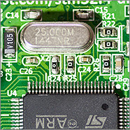
It all ended well and here’s a picture of the new crystal in-place on the board.
Testing the board
I’ll be using my stm32plus library to test the board. The first quick-and-dirty test is to blink a LED at 1Hz. The source code is below.
// initialise the pin for output

GpioD<DefaultDigitalOutputFeature<13> > pd;

// loop forever switching it on and off with a 1 second
// delay in between each cycle

for(;;) {

  pd[13].set();
  MillisecondTimer::delay(1000);

  pd[13].reset();
  MillisecondTimer::delay(1000);
}
The MillisecondTimer class relies on the ARM core SysTick peripheral for timing, which itself is fed from the MCU core clock, which in turn is generated by the PLL from a set of multipliers and dividers that operate on the incoming X2 signal.
I set those multipliers/dividers up to generate a core frequency of 168MHz from an assumed 25MHz oscillator. If the actual incoming frequency is not 25MHz then the knock on effect is that SysTick will not tick at the expected 1ms and my LED will not blink at 1Hz.
It’s a quick-and-dirty low resolution test, but it works. And it did work. And that means that my incoming frequency is at or close to 25MHz.
Pingback: Swapping Dev Board Crystals to Suit Your Needs - zeax blog (ze-ax.com)()