


ST-Link v2. One programmer for all STM32 devices
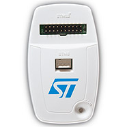
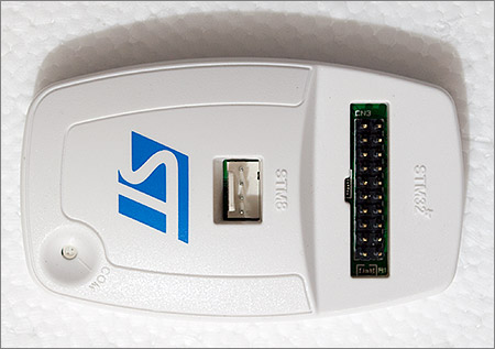
Over the last few years I’ve amassed quite a collection of STM32 development boards. Third party boards dominate my collection for the F1 series whilst I have official ST discovery boards for the F0, F4 and F1 Value Line. We’ve been lucky with the official ST discovery boards because they all come with an ST-Link included on the PCB so you don’t need to buy anything else at all to get a complete C++ development and visual debugging environment up and running.
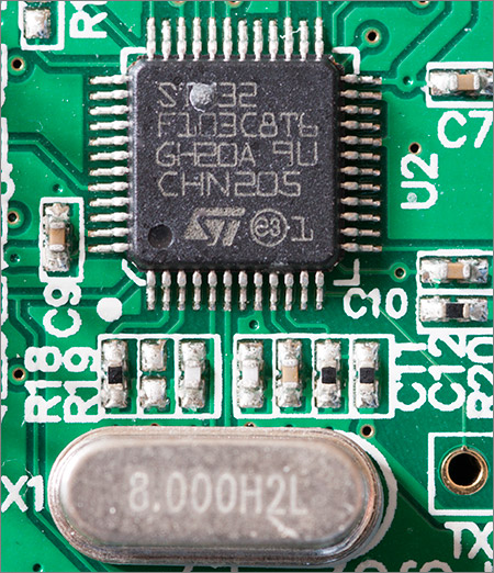
The embedded ST-Link debugger on the discovery boards is implemented inside ST’s own STMF32F103C8T6 MCU in a 48 pin QFP package with an external 8MHz clock. I suppose that when you are the manufacturer of these MCUs it’s cheaper to do it this way than to manufacture a custom ST-Link IC just for this purpose
The situation with the commonly available third party F1 boards was always less clear because up until a year or so ago the ST-Link interface was not fully operational in the popular and free OpenOCD debugger. Because of the lack of support in OpenOCD for ST-Link v2 I was forced to go down the third party route and use the Olimex ARM-USB-TINY-H for all my F1 programming and debugging.
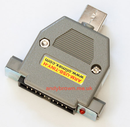
This is a JTAG-based programmer that is compatible with ARM devices from many manufacturers. It’s fast, reliable and it costs double what you should be paying for an ST-Link v2.
Times have changed since those early days and now since the release of version 0.7.0 of OpenOCD the support for ST-Link is completely stable and there’s no reason why you can’t use ST-Link v2 for all your STM32 programming and debugging needs.
Not only is it the most compatible of all the programmers and debuggers, it’s also probably the cheapest. At the time of writing it’s only £18.68 plus VAT at Farnell. If you’re buying elsewhere then make sure that you’re getting the ‘v2’ device. There are still some places offering the older ‘v1’ version.
In the rest of this article I’ll take each board that I’ve got and explain how to connect and use it with OpenOCD using the ST-Link v2 programmer. Once you’ve got a live OpenOCD connection you can flash your .hex binaries and do interactive debugging using Eclipse.
The version of OpenOCD that I’ll be using is 0.8.0 and my test system will be Windows 7 x64 using Cygwin. The OpenOCD binaries were downloaded from Freddie Chopin’s site.
If you’re installing OpenOCD for the first time on Windows then you’re likely to run into an issue with the libusb package that shows up as the following error:
Open On-Chip Debugger 0.8.0 (2014-04-28-08:42)
Licensed under GNU GPL v2
For bug reports, read
        http://openocd.sourceforge.net/doc/doxygen/bugs.html
srst_only separate srst_nogate srst_open_drain connect_deassert_srst
Info : This adapter doesn't support configurable speed
Error: libusb_open() failed with LIBUSB_ERROR_NOT_SUPPORTED
Error: open failed
in procedure 'transport'
in procedure 'init'
To resolve this, download and run the zadig utility. Zadig automates the process of connecting libusb to one of the supported USB drivers. It’s as simple as a single click.
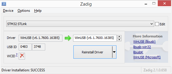
Once zadig has done its work you can run OpenOCD again and it’ll work this time.
STM32F103VET6 ‘Mini’ board
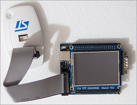
This was the first F1 development board that I bought some years ago and it’s still available in various forms on ebay. Connectivity with the ST-Link device is via a direct connection to the 20-pin JTAG/SWD header using the supplied cable. Since the ST-Link connection is not designed to supply power to the target board you must also connect up the USB A-B cable.
Here’s the command sequence for connecting with OpenOCD:
$ pwd
/cygdrive/p/docs/cyghome/andy/openocd-0.8.0
$ bin-x64/openocd-x64-0.8.0.exe -f scripts/interface/stlink-v2.cfg -f scripts/target/stm32f1x_stlink.cfg
Open On-Chip Debugger 0.8.0 (2014-04-28-08:42)
Licensed under GNU GPL v2
For bug reports, read
        http://openocd.sourceforge.net/doc/doxygen/bugs.html
Info : This adapter doesn't support configurable speed
Info : STLINK v2 JTAG v17 API v2 SWIM v4 VID 0x0483 PID 0x3748
Info : using stlink api v2
Info : Target voltage: 3.225049
Info : stm32f1x.cpu: hardware has 6 breakpoints, 4 watchpoints
‘Redbull’ STM32F103ZET6 board
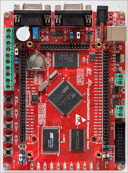
This is my favourite F1 development board. It’s based around the full fat STM32F103ZET6 144-pin MCU and comes with additional SRAM and flash resources as well as the usual buttons and LEDs. On my board the additional SRAM and flash ICs are the ISSI IS61LV256160AL-10TL, the SST 39VF1601 and the Samsung K9F1G08U0C. These are correctly mapped to the MCU’s FSMC peripheral as you’d expect. My only minor gripe with the board is that there’s not enough exposed GND and 3.3V pins for hassle-free connecting of external peripherals.
Connecting the board with ST-Link is identical to the ‘Mini’ board described above. Simply connect it up to the 20-pin JTAG header and run the same command sequence:
$ pwd
/cygdrive/p/docs/cyghome/andy/openocd-0.8.0
$ bin-x64/openocd-x64-0.8.0.exe -f scripts/interface/stlink-v2.cfg -f scripts/target/stm32f1x_stlink.cfg
Open On-Chip Debugger 0.8.0 (2014-04-28-08:42)
Licensed under GNU GPL v2
For bug reports, read
        http://openocd.sourceforge.net/doc/doxygen/bugs.html
Info : This adapter doesn't support configurable speed
Info : STLINK v2 JTAG v17 API v2 SWIM v4 VID 0x0483 PID 0x3748
Info : using stlink api v2
Info : Target voltage: 3.272160
Info : stm32f1x.cpu: hardware has 6 breakpoints, 4 watchpoints
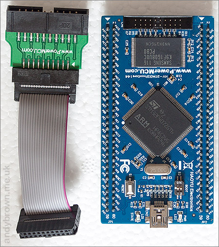
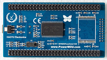
PowerMCU STMF407ZGT6 board
Making an entry into the F4 development board business can’t be easy when ST sell the discovery board for such a low price. Therefore any competitor is going to have to offer significant extras to have any hope of selling their board.
This development board offers several nice upgrades to ST’s discovery offering. Firstly the MCU is the 144-pin device which means that all banks of the FSMC peripheral are available and this board builds on that by including a Samsung K9F1G08U0C NAND flash chip on the front side of the board.
Note that the external clock is 25MHz which means that a straight recompile of firmware that targets the discovery board will not be enough. You will need to go into the startup code and set the appropriate PLL multipliers to get the clock tree set up correctly. ST provide an Excel spreadsheet with macros that will do this for you – search for AN3988 to get it.
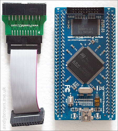
I can’t finish up with the front side of this board without having a moan about the JTAG/SWD header. It’s a reduced size 2mm pitch socket that requires an adaptor to connect to the standard 2.54mm JTAG header. I can’t seriously believe that it was cheaper to save a few millimeters of board space than it was to ship a cable adaptor with every board as they do. Barmy decision.
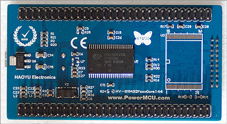
I need to show the back of the board because there’s a few significant components down there. The large IC is a Cypress CY62157EV30L SRAM device, correctly connected to the MCUs FSMC peripheral. The unpopulated footprint looks like it was originally designed to hold a NOR flash IC but is unpopulated on my board.
I’m pleased to see the linear regulator is an AMS1117 3.3V device. This a much more heavy duty regulator than the one on the discovery board and will allow you to connect more demanding peripherals than you can attach to the discovery board.
And so on to the OpenOCD connectivity. Hook up your standard JTAG cable to the board via the adaptor supplied with the board and here’s how to attach to it:
$ pwd
/cygdrive/p/docs/cyghome/andy/openocd-0.8.0
$ bin-x64/openocd-x64-0.8.0.exe -f scripts/interface/stlink-v2.cfg -f scripts/target/stm32f4x_stlink.cfg
Open On-Chip Debugger 0.8.0 (2014-04-28-08:42)
Licensed under GNU GPL v2
For bug reports, read
        http://openocd.sourceforge.net/doc/doxygen/bugs.html
Info : This adapter doesn't support configurable speed
Info : STLINK v2 JTAG v17 API v2 SWIM v4 VID 0x0483 PID 0x3748
Info : using stlink api v2
Info : Target voltage: 3.217755
Info : stm32f4x.cpu: hardware has 6 breakpoints, 4 watchpoints
PowerMCU STMF207ZGT6 board
This entry into the F2 development board market is from PowerMCU.com and it’s pretty much identical to the F4 board that I described above, including the external 25MHz crystal that will require some attention in your code if you’re already working with something that assumes an 8MHz crystal.
All the additional features on this board are identical to those on their F4 offering so I won’t repeat them here.
The back side of the board yields no surprises having already seen the F4 board. Let’s move quickly on to the OpenOCD commands to connect to it:
/cygdrive/p/docs/cyghome/andy/openocd-0.8.0
$ bin-x64/openocd-x64-0.8.0.exe -f scripts/interface/stlink-v2.cfg -f scripts/target/stm32f2x_stlink.cfg
Open On-Chip Debugger 0.8.0 (2014-04-28-08:42)
Licensed under GNU GPL v2
For bug reports, read
        http://openocd.sourceforge.net/doc/doxygen/bugs.html
Info : This adapter doesn't support configurable speed
Info : STLINK v2 JTAG v17 API v2 SWIM v4 VID 0x0483 PID 0x3748
Info : using stlink api v2
Info : Target voltage: 3.238120
Info : stm32f2x.cpu: hardware has 6 breakpoints, 4 watchpoints
Cheap ST-Link clones
Recently there have been a number of bare boards appearing on ebay for as little as £5.00 that claim to function as ST-Link v2 devices. They’re so cheap that I thought I’d pick one up and see what the story is.
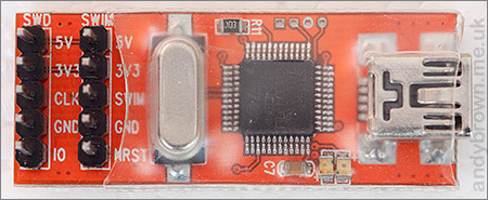
My first observation is that I can’t see how these things are legal at all. Apart from the obvious unauthorised use of the USB VID and PID that belong to ST Microelectronics there is the question of the firmware implementation itself. If you look closely at an official ST discovery board then you’ll see that ST-Link is implemented in firmware inside an STM32F103 device. The exact same model of STM32F103 appears on this clone. I can only surmise that the manufacturer has somehow managed to circumvent ST’s code readout protection (assuming that ST remembered to enable that protection) and cloned the firmware byte for byte.
Does it work though? Let’s try it out and see. I’m going to refer to it as the FakeLink from here on just so you know that’s the one I’m using. I hooked it up to the ‘RedBull’ F1 board using jumper wires connected from the FakeLink to the JTAG socket using the following pinout. GND -> GND(4), 3V3 -> board 3V3, CLK -> SWCLK(9) and IO -> SWDIO(7).
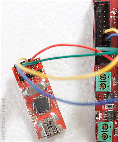
For the tests I connected just the FakeLink USB connector to the computer. It seems that the FakeLink can power the dev board from its 3.3V output. I also tested it with the dev board receiving power from its USB connector and the results were the same.
Now let’s pretend it’s a real ST-Link and connect to it via OpenOCD.
$ bin-x64/openocd-x64-0.8.0.exe -f scripts/interface/stlink-v2.cfg -f scripts/target/stm32f1x_stlink.cfg
Open On-Chip Debugger 0.8.0 (2014-04-28-08:42)
Licensed under GNU GPL v2
For bug reports, read
        http://openocd.sourceforge.net/doc/doxygen/bugs.html
Info : This adapter doesn't support configurable speed
Info : STLINK v2 JTAG v17 API v2 SWIM v4 VID 0x0483 PID 0x3748
Info : using stlink api v2
Info : Target voltage: 3.560727
Info : stm32f1x.cpu: hardware has 6 breakpoints, 4 watchpoints
So far so good though the target voltage is higher than I would have expected. Next I’ll try the basic functionality and flash a ‘blink’ example to the MCU using telnet to control the connected OpenOCD server.
$ telnet localhost 4444
Trying 127.0.0.1...
Connected to localhost.
Escape character is '^]'.
Open On-Chip Debugger
> reset init
target state: halted
target halted due to debug-request, current mode: Thread
xPSR: 0x01000000 pc: 0x08000238 msp: 0x2000fffc
> flash write_image erase p:/tmp/blink.hex
auto erase enabled
target state: halted
target halted due to breakpoint, current mode: Thread
xPSR: 0x61000000 pc: 0x2000003a msp: 0x2000fffc
wrote 8192 bytes from file p:/tmp/blink.hex in 0.771045s (10.376 KiB/s)
> reset
The first command, reset init resets the MCU and brings it under the control of OpenOCD. The next command, flash write_image erase p:/tmp/blink.hex writes the compiled blink program to the MCU and finally we reset it to run the program with reset.
It worked as expected. So far so good for the FakeLink. Now for the only test that really matters, can I debug the program from Eclipse just like I can with the real ST-Link? People often write to me asking for the Eclipse debug settings that I use, so here they are:
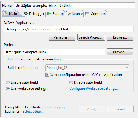
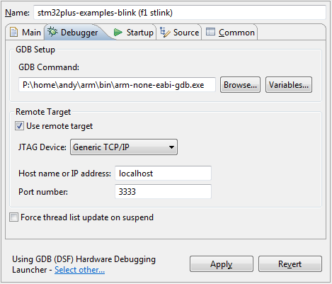
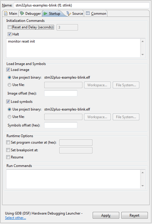
Executing the debug configuration resulted in everything working just as I would expect it to. Eclipse was able to auto-flash the compiled executable and then set breakpoints and single step through the code. Basically it just worked.
Verdict on the fake ST-Link
Functionally the device passed every test that I executed so in that respect I have to give it a plus mark. However, I just can’t condone the blatant illegality of the thing. It is an unashamed rip-off of ST’s intellectual property as well as the PID/VID owned by ST. In my view, especially as the offical ST-Link not expensive, the right thing to do is to buy the ST device and don’t support these clones.