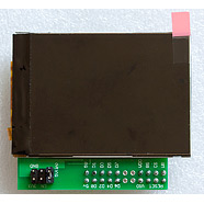
Nokia N82 2.4 inch QVGA TFT on the Arduino
It’s been a few months now since I released the original two articles that detailed the design, build and optimised software library for the 2.0″ Nokia 6300 QVGA TFT connected to the Arduino Mega XMEM interface. Judging by the responses I’ve had, there’s a lot of you out there that are interested in connecting these mobile phone TFTs to your Arduinos.
Today we move on to reverse-engineer another Nokia QVGA TFT. This time we’re going to tackle the Nokia N82. Read on to find out how I got on.
The N82 TFT
The N82 TFT is a 2.4″ panel that’s also found in the N77, N78, N79, E66, E52, E75 and 6210S. It’s certainly clear that back in the not-so-distant past when Nokia was the clear market leader in mobile phones they certainly knew how, as a company, to take a successful design and keep re-releasing it over and over again with small tweaks to keep the income rolling in. Replacement N82 panels are available at the time of writing for as low as £3 on ebay.
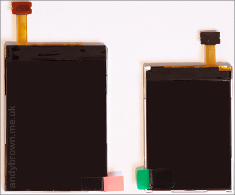
Two TFTs. The N82 next to the 6300.
You can get an idea of the physical size difference between the 2.4″ and 2.0″ panels from the above photograph. The resolution is identical, the pixels are simply larger on the N82 panel. Pixel densities are around 200ppi for the 6300 and 167ppi for the N82. Having a higher pixel density means that your graphics appear smoother. Having a lower pixel density makes your text larger, and perhaps more readable.
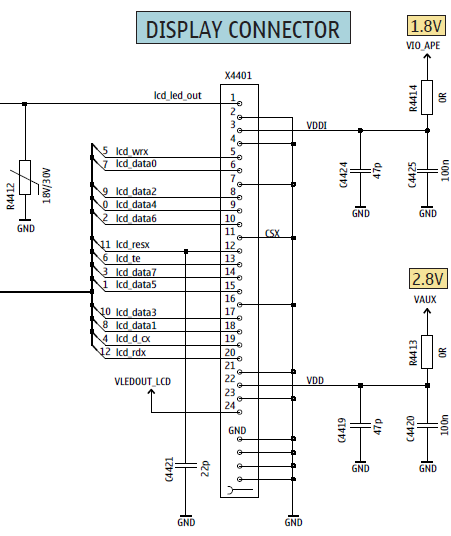
The schematic and the connector
It must be our lucky day because the pinout to the N82 is identical to the 6300 and it uses the same 24-pin board-to-board connector too! The 0.4mm pitch connector is made by JST and the part number is 24R-JANK-GSAN-TF. Here’s the datasheet.
It is easy to obtain them either direct from JST’s online shop or in small quantities from online sources. Here are some direct links to the ones that I know of:
gsmserver.com
cellnetos.com
stellatech.com
The pinout for the connector is shown here:
Here’s a photograph of the connector plug. If you look closely you can see where the ground pins connect directly into the ‘ground pour’ inside the ribbon cable. This helps to identify where pin 1 is located when doing the reverse engineering.
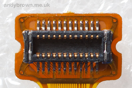
The connector on the LCD FPC cable
The backlight
The backlight shares the same design as the 6300 in that it consists of four white LEDs in series. Therefore we will use the same NCP5007 constant current LED driver from OnSemi that we’ve been using in all our Nokia TFT designs so far.
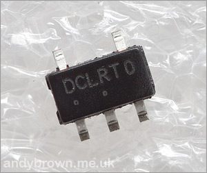
The NCP5007 in SOT23-5 package
The NCP5007 will be configured to supply a constant 20mA through the backlight circuit and we will use a PWM signal on the ENABLE pin to vary the brightness. The NCP5007 really is a wonderful little device – truly one of those things that ‘just works’ and I’ll use it wherever I need to drive up to 5 LEDs.
The development board schematic
We’ll gloss over the explanation of how we drive the TFT controller using the Arduino Mega XMEM interface because that’s all been explained in this article and there are no changes to the interface in this design.
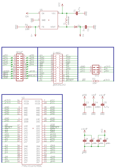
The Eagle schematic, click to download a PDF.
Just as before, we choose to use the 74ALVC164245 16-channel level converter from NXP to handle the conversion of the 5V signals from the Arduino down to a safe level of 3.3V where they won’t damage the panel.
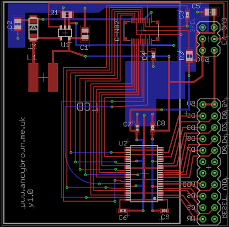
The Eagle PCB design, click for larger.
In this design I’m using the TSOP-48 (0.5mm) pitch version of the level converter rather than the SSOP-48 (0.635mm) pitch that I used in the 6300 design. The reason for the change is that the TSOP-48 package is more readily available from the suppliers that I use.
Another slight change, again due to parts availability, is the inductor. I’ve switched to a slightly different model that has a larger footprint but is otherwise functionally identical to the one I was using before.
Bill of Materials
Here’s a full list of parts used in this development board.
| Part | Value | Device | Package |
|---|---|---|---|
| C-N82 | NOKIA12X2 | 24R-JANK-GSAN-TF | 12X2 |
| C1,C5 | 4.7µF | ceramic | 0805 |
| C2 | 1µF | ceramic 50V | 0805 |
| C3,C4,C6,C7,C8,C9 | 100nF | ceramic | 0603 |
| D1 | Diodes Inc. BO530W-7 | schottky | SOD-123 |
| L1 | Sumida 22µH | CDRH5D28NP-220NC | 6x6mm |
| MEGA | pin header | MA12-2 | MA12-2 |
| R1 | 10Ω 1% | resistor | 0805 |
| R3 | 33KΩ | resistor | 0805 |
| SV2 | pin header | MA03-2 | MA03-2 |
| U1 | NCP5007 | NCP5007 | SOT23-5 |
| U2 | 74ALVC164245DGG | level converter | TSOP48 |
The development board
I generated the Gerber’s from Eagle and sent them off to ITead Studio to be printed using their very good value prototype PCB service. A few weeks later they arrived and all were perfect, just as I’ve come to expect.
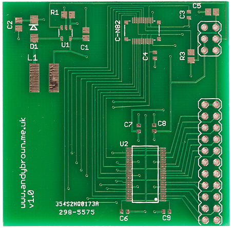
The front of the PCB. The pads are not gold, the tungsten lighting used in the photograph just makes them look like they are.
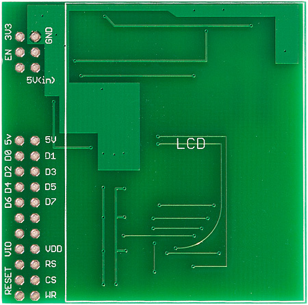
The back of the PCB
Building the board is a familiar process for me by now. In case you’re interested, this is the procedure that I follow.
- Flux the pads then tin them with an iron so they all have little solder bumps on them. For the level converter and the connector this means loading up the tip of the iron with solder and lightly dragging it over the pads.
- Use a very small amount of paste flux as a glue to hold down the level converter, connector and inductor in place on the board. Overdoing the flux can cause bubbling during the reflow which will cause the component to move out of position (very bad).
- Heat the board with the three parts on a hot-plate until the solder reflows and the parts sit down into position.
- Inspect the joints under a microscope and use a fine-tip iron to touch each one that shows any movement when prodded with a pin. There will be at least one…
- Use tweezers and a hot-air gun to reflow the other components into place.
- Clean the board with soapy water and a toothbrush then leave for at least 24 hours in the airing cupboard to dry out.
- Solder the 2.54mm headers and test.
So it’s not a short process but the rewards are worth the effort. Here’s the fully built development board.
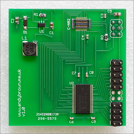
The board, fully built and awaiting the LCD
And here’s a shot with the LCD fitted. The 2.4″ display is a little oversized for the PCB but fits firmly and saves the additional cost of the larger PCB just to mount the screen.
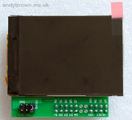
The board with the LCD attached.
Driver source code
My XMEM driver code has been updated to include support for the N82. You will need to download at least version 2.1.0 of the driver to get that support.
Because the panel is driven identically to the Nokia 6300, all the examples will work as-is with no changes. However, for completeness I have included “N82” driver names just in case I need to create specific customisations for this panel in the future.
#include "NokiaN82.h"

using namespace lcd;

typedef NokiaN82_Portrait_262K TftPanel;
The example snippet shows the driver name (NokiaN82_Portrait_262K ) and the header file (NokiaN82.h). Similar driver names for the Landscape orientation and 16M and 64K display modes (if supported by the panel) are included.
Another example
I created a full example that exercises the compressed graphics capability of the driver in a simulation of the output from a weather station on the Arduino. The source code is included in version 2.1.0 and above of the software driver.
This demo packs in 100Kb of compressed graphics in to the Atmega1280 and the controller code takes up a further 10Kb or so. The graphics are decompressed on-the-fly from flash by my LZG decoder routine included with the driver.
Here’s a video of the demo in action. Watch it here or click to watch in HD at YouTube.
Copyright Notices
The graphical weather images were downloaded from the Wikimedia Commons library. Please respect the rights of the original authors:
Snow image
Partly cloudy image
Rain image
Sun image
The numeric ‘temperature readout’ was created by typing the numbers 0..9 and the point and degree symbols into Wordpad in a nice font at 48 point size. Then I took a screenshot and used a paint program to crop out each character into its own bitmap and saved each one as a separate PNG.
I then ran the bm2rgbi utility included with the graphics library to convert the PNGs to LZG format and imported those binaries directly into the compiled flash image. You can see how that’s done by reading the example source code.
JPEG support now available
I’m pleased to announce driver support for displaying JPEG images. JPEG images may be compiled into flash and displayed from there or they may be streamed over an Arduino serial connection.
The driver documentation has been updated to include sample code and a demo video that shows you how to do it.
Here’s a link to the video that shows the JPEG decoder operating on images stored in flash. If you’d like to see it operating on JPEG images received over the serial link then please refer to the main driver documentation. The JPEG decoder is completely compatible with the Nokia 6300 as well as the N82.
Can I use it with the standard Arduino?
Yes you can, see this article for a write-up, including performance analysis and optimisations. The article is focused on the 6300 but the N82 works in exactly the same way.
Update: 23 September 2012
Another controller variant has turned up and we’re going to call this one ‘Type C’. It’s showing up in both 6300 and N82 screens. It behaves the same as Type A screens except for the following differences:
- It won’t go into BGR colour transfer mode, only RGB is supported. Since RGB is supported by all variants I’ve seen RGB will become the default mode in my driver code from 2.2.0 onwards.
- Page and column addresses are not reversed in landscape mode.
Type C panels are supported from version 2.2.0 of my driver code using a _TypeC suffix to the driver name. e.g. Nokia6300_Landscape_262K_TypeC.
Print your own PCBs
Want to try assembling a board yourself but don’t have a home-etching kit? No problem, just download the Gerber files from my downloads page and use an online prototyping service such as that offered by Seeed Studio, ITead Studio or Elecrow.

