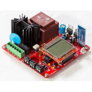
An android reflow controller that anyone can build

The story so far

Welcome to the never ending saga of Andy and his reflow controllers. About a year ago I published a project writeup showing how I built a PID-based reflow controller. It featured a 640×360 graphical LCD from the Sony U5 Vivaz mobile phone and was all-surface mount. It worked well and continues to serve me well to this day but I always thought that there were improvements that I could make in several areas.

Firstly, there’s no reason why it should have been all surface-mount. The LCD in particular has a 0.4mm connector that many people will find very hard to solder by hand. After all, presumably you’re building a reflow controller to help solve that very problem. Chicken and egg.


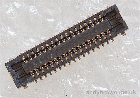
Difficult 0.4mm connector

Secondly, the built-in LCD is overkill. We live in the age of the so called landfill android device where you can buy a powerful tablet computer for just Β£30 online. Why not harness that power and use bluetooth to transmit a control protocol back and forth to a simple on-board controller?
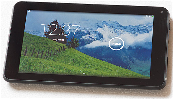

7″, 1024×600 IPS, bluetooth. Β£35 delivered.

Finally, I used an SSR to pulse the oven power supply on and off. That always irked me. A fully integrated controller would be supplied by the mains and use zero-crossing detection to drive a triac that would dim the halogen oven instead of just switching it on and off.

A few months ago I set to work solving all these issues and I’m happy to say that they’ve all been addressed. In the remainder of this article I’ll present a reflow controller that’s almost entirely through-hole so anyone can build it. It’ll be driven direct from the mains supply and will feature bluetooth control via an Android app.

The schematic

Let’s get straight into the schematic. This is a modular design so I’ll pick on each part individually and explain what’s going on. Here’s the full document.
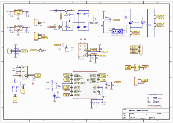


Click image for PDF

This design is for countries with a 220-240VAC supply. I have estimated some of the values that I consider to be appropriate for countries with a 120VAC supply and they are shown in red on the schematic but I haven’t tested these and would appreciate any corrections from people in those countries.

The high-side of the board

MAINS_L and MAINS_N are the live and neutral mains terminals, respectively. SW_IN and SW_OUT are the terminals that connect to the on-off switch. The maximum current rating for this design is 8A so the switch must be rated accordingly and should contain an embedded fuse because there’s no provision for one on the board itself. There’s not much chance of a standard household fuse blowing before the triac is destroyed but it should blow before anything really bad, such as a fire, starts.

C4 is an X-class film capacitor rated at 275VAC. It’s used for emissions filtering and can be considered optional if you’re not bothered about that.

You have your fuse for overcurrent protection and now you have R3, a varistor for overvoltage protection. Under normal operating conditions the varistor has a very high resistance but when a voltage spike is encountered the varistor quite suddenly becomes very low resistance, protecting the triac from the spike. I’ve never personally witnessed a triac failure but I’m informed that they can fail explosively so it’s good to protect them if we can.

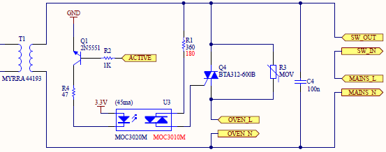
OVEN_L and OVEN_N are the live and neutral output terminals to the halogen oven. The triac controls when these terminals are switched on and off. Speaking of the triac…

The triac

Q4, R1, U3, Q1, R2 and R4 form the triac control circuit and it’s worth exploring this in a little more detail.

A triac is an electronically controlled semiconductor that, when activated, can conduct current through it in either direction. This bi-directionality makes it a good choice for using a small DC control signal to switch a large AC mains supply on and off. Another key feature is that once a triac is activated (latched) it will stay latched on until the AC sine wave crosses zero again. If we combine this feature with a zero-crossing detector then it becomes a simple matter of timing to ‘dim’ an AC wave by chopping it off at the same point in each half-cycle.


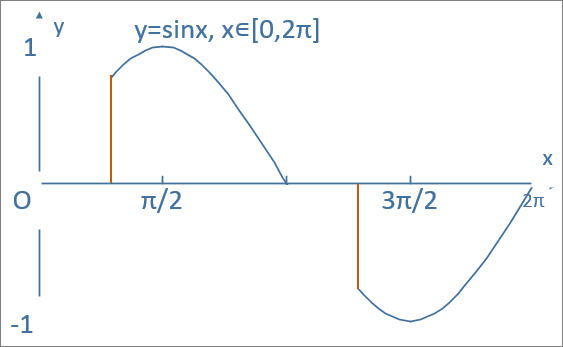
Chopped (dimmed) AC waveform

The diagram above shows an example of how AC dimming is achieved. You wait until the wave crosses zero, then you wait some more depending on how little or how much dimming you want and then you switch on the triac. The triac will then stay switched on until the next zero crossing at which point you start again.

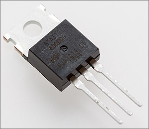
It’s important to choose a triac that’s rated comfortably in excess of the current that you plan to conduct so that it can handle the inrush current surge that happens when the halogen oven first switches on. I rate this controller for an 8A load so I’ve chosen a BTA312-600B 12A triac from NXP to do the job. Note as of 2017 this Triac is now obsolete. Replace it with the directly equivalent ST Micro BTA12-600BWRG.


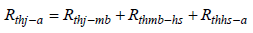
The TO-220 package can be cooled in accordance with the rating of the BTA312.

A triac of this size will typically come in a TO-220 package and it will get hot during use so an appropriately rated heatsink is absolutely required.


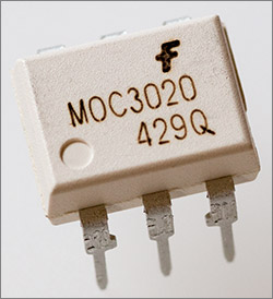
Fairchild MOC3020M in an on-trend white package

I use a MOC3020M triac optocoupler to control the triac’s gate and the driving circuit is taken from the MOC3020M datasheet with the RC snubber components removed. A snubber is used to prevent false triggering of the triac when the load being driven has an inductive component such as the fan on the halogen oven that I’m using. False triggering tends to happen during the 4th triac quadrant and can be eliminated by using a triac that only triggers in quadrants 1 to 3, such as the BTA312 that I’m using. Therefore I don’t need an RC snubber and have removed it from the circuit.

The MOC3020M requires between 30 and 60mA to switch on. This is too much to drive directly from the pin of an MCU so I’m using the 2N5551 transistor, Q1, to drive it. There’s nothing special about the 2N5551, I just happen to have some in stock. If you have another general purpose NPN knocking around then you can use that. Just be sure to choose a base resistor that fully switches the transistor on.

Triac thermal considerations

I mentioned before that a triac can get hot and we need to provide them with at least a heatsink and sometimes even a fan for active cooling. Heatsinks are rated in °C/W which tells you how many degrees they will rise above ambient per Watt of thermal energy that you ask them to dissipate.

NXP publish a helpful and well-written application note that walks you through the maths required to calculate the power dissipated by the triac.

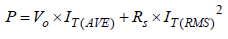
P is the power dissipation in Watts, V0 is the triac’s knee voltage, given in the datasheet. IT(AVE) is the average load current and is calculated from the RMS load current using the following equation:

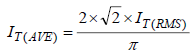
RS is the triac slope resistance and can be found in the datasheet. Referring to the BTA312 datasheet we find V0 = 1.164 and RS = 0.027. I’ll use IT(RMS) of 8A as the worst case for this design. Using the second equation I calculate that IT(AVE) = 7.2A. Now I can use the power equation to determine that P = 10.1W. I’ll definitely need a heatsink.

Choosing a suitable heatsink

Tj is the triac’s junction temperature and it must be kept below the maximum value specified in the datasheet: 125°C for the BTA312 and in practice we need to stay well away from that value due to the error margin between the theoretical thermal calculations and real life.

AN10384 gives us the equation that we need to calculate the junction temperature for the power dissipation that we have just calculated.

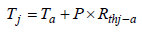
Ta is the ambient temperature (°C) and Rthjβˆ’a is the junction-to-ambient thermal resistance (°C/W). The package’s Junction-to-ambient will often be quoted in the datasheet and can be used to determine if you can operate your design without a heatsink. It is 60°C/W for the BTA312’s TO-220 package which means that I must definitely use a heatsink.

Thermal resistance, like electrical resistance, can be broken down into several smaller resistances connected in series. The TO-220 package used by the BTA312 has the following resistance model:

See figure 3 in AN10384 for a pictorial representation of where the different components of the overall thermal resistance occur in the TO-220 package.

Rth j-mb is the thermal resistance of the junction to mounting base. The value is quoted in the datasheet as 2°C/W for a half-cycle.

Rth mb-hs is the resistance between the mounting base of the TO-220 and the heatsink. This will vary depending on whether the package is screwed or clipped to the heatsink and whether or not thermal grease is used. I am screwing the TO-220 to the heatsink and I will use thermal grease. AN10384 quotes a typical value of 0.5°C/W for this method.

Rth hs-a is the resistance between the heatsink and ambient and will be quoted by the manufacturer. I’ve now got enough numbers to work out the maximum thermal resistance that I can accept from my heatsink. If I assume that I don’t want the junction temperature any higher than 100°C then the maximum heatsink thermal resistance works out to be 5°C/W.

I had a browse through the range of TO-220 heatsinks at Farnell and found that the FA-T220-38E offers a thermal resistance of 3.8°C/W in a nice compact unit.


Ohmite FA-T220-38E heatsink

Putting the rating of 3.8°C/W into the Tj equation yields a value of 88°C for an ambient temperature of 25°C. This value will rise by 1°C for every degree rise in ambient. I’m happy with that value and will definitely use this heatsink in my design.

The transformer

In the interests of safety I decided to use an isolation transformer to step down the mains voltage to a safe level for the low side of the board. Transformer-less designs for powering MCUs from the mains do exist and are cheaper to build but they are not as safe.

The Myrra 44193 steps down a 220-240VAC input to a 6VAC output with full isolation protection. The coils are encased in an insulating material and you can’t see it but there will be a piece of insulating material between the two coils to prevent accidental short circuit. Finally the whole unit is potted with some kind of resin. It’s a very heavy component and certainly feels well made.

The mains connector

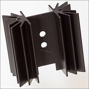
The mains connector block is a 6-way 5.08mm connector designed to handle all the mains inputs and outputs. Two pins are provided for 240VAC live and neutral. Two similar pins are provided for the oven output and two more pins are provided for routing out to an external on-off switch.

I’ve chosen an appropriately rated connector block that you can get from Maplin (order code A18QN). You could use screwed down spade connectors instead if you’re unable to obtain a suitable connector in your country. Directly soldering mains wires to a PCB is generally not recommended because stress over time can result in a cracked joint.

I’ll be running a 3-core cable to the metal housing that I use to enclose the PCB. The earth wire will be screwed to the metal housing as will the metal mounting screws for the project PCB that will also connect to the ground plane on the low-side of the device.

There was no room to mount a fuse on the PCB so the IEC connector that I will mount to the chassis of the enclosure has a fuse holder built in to it.

The low-side of the board

Now we’re done with the mains stuff, let’s move on to the low-side of the board, starting with the bridge rectifier and zero-crossing detection circuits.


Bridge rectifier and zero-crossing detector

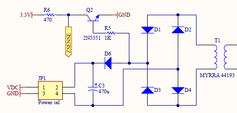
The output of the transformer is a sine wave, shown below:

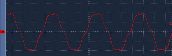
Diodes D1 to D4 form a classic full wave bridge rectifier circuit used to turn the negative part of the wave into positive.


Full-wave rectified output

I used 1N4007 diodes for the rectifier which, with their 1kV rating are very much over-specified for this purpose. I used them simply because I had a lot of them in stock. You can just as easily use any of the others from the 1N400x range if that’s what you have available.

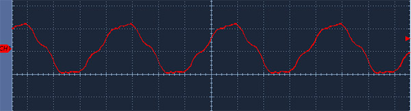
Capacitor C3 is used to smooth the rectified wave into something that we can sensibly use for input to the LDO regulators that will supply 5V and 3.3V to the rest of the board. Diode D6 shields the zero-crossing detection circuit from the effect of the smoothing capacitor.


Smoothed output

The scope’s voltage scale is 2V/div in the above screen shot so we can see that I’m getting around 6.5V which is enough to power the LD1117 5V regulator with its 1V (typical) drop-out. The capacitor C3 can’t completely smooth the output on its own which is why there’s an apparent sawtooth ripple to the output. Let’s have a look at that ripple magnified:


Magnified ripple

My scope shows that the peak-to-peak ripple voltage is about 1.2V, quite a lot really and we’ll have to see how that affects the output from the regulators, particularly the 3.3V regulator that powers the thermocouple A-D converter.

R5, R6 and Q2 form the zero crossing circuit. What we aim to do is convert the rising and falling AC wave into a digital on-off signal that we can use as an input to an MCU pin. We can then use the MCU’s ability to raise an interrupt on the rising or falling edge of a signal to tell us when the zero crossing has happened.


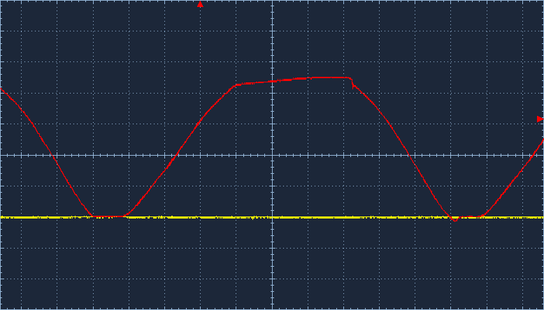
Scope probe of the AC wave and the ZSENSE pin level

The AC wave is applied through a base resistor to the 2N5551 general purpose NPN transistor. When the wave rises past the base-emitter ‘turn-on’ voltage of the transistor then it will conduct and the ZSENSE pin will sense zero since the transistor is now allowing current to flow through it to ground. When the wave falls below the ‘turn-on’ voltage the transistor will stop conducting and the ZSENSE pin will read high. The falling edge happens close enough to the zero crossing for me to use as a signal to start my triac activation timing calculations.


On/off switching for different percentages

This animated image shows the ACTIVE signal in relation to different dimming percentages from zero to 100 in steps of 10. For the 100% signal I just set the line high and for zero it is set low.

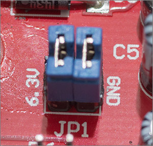
The JP1 jumper is my way of safely working on the low-side of this board without having to connect it to the mains. The normal case is for the jumpers to be fitted and the low-side is then powered by the mains. When I’m working on it I remove the two jumpers and connect my bench DC power supply to pins 1 and 3.

Voltage regulation

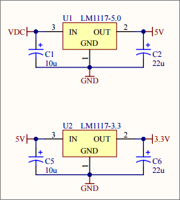
The roughly 6.3V output from the bridge-rectifier is fed to a pair of ST Micro LD1117 regulators in TO-220 packages. I would have liked to have had the whole board running at 3.3V but unfortunately the HC-06 bluetooth module has a bizarre power arrangement whereby the signal levels are specified to be at 3.3V but the adaptor board takes a 5V power input. That’s annoying but LD1117 voltage regulators are cheap and I’ve got the board space so it’s no problem to take two.

I haven’t measured the noise levels on the regulator outputs in isolation – only with the full board built and with no issues observed in the prototype I can only assume that the outputs are stable enough for this design.

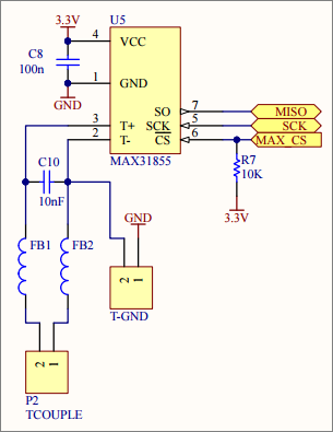
The thermocouple ADC

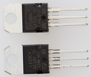
In my previous design I elected to use the older MAX6675 K-type thermocouple ADC. That chip is now obsolete, replaced by the pin-compatible MAX31855 that adds a few new features, the most notable of which is the ability to measure below zero. Firmware written for the MAX6675 will need to be re-written for the MAX31855 but the differences are minimal and it’s still the same old poll-over-SPI protocol.

Bad Max 2

I am beginning to lose faith in Maxim’s ability to produce things that work. Readers of my previous article will remember that I managed to get hold of a bad MAX6675 that caused me to lose hours of my life trying to figure out what was wrong before figuring out that the IC itself was bad.

Well it happened again with the MAX31855. This time the symptoms were an incorrect scaling as the temperature rose. That is, it would appear to be correct at room temperature but would then lag as the temperature increased. For example, dunking a waterproofed thermocouple probe in boiling water would read around 75°C when the real temperature is obviously 100°C. Having been burned before by dodgy Maxim gear I googled around and stumbled across this article on the eevblog forum. Exactly the same symptoms as me and yes, I had a MAX31855 with one of the date codes identified as dodgy.
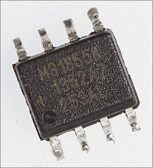

253AL date code

So if you’ve got a MAX31855K with this date code then don’t even bother trying to fit it. Toss it in the bin or return it to your supplier and get a replacement.

The replacement that arrived worked perfectly. No more dodgy temperature readings. After all these less than ideal experiences I’m tempted to drop the whole K-type thermocouple approach and use an RTD instead.

The two ferrite beads and the 10nF capacitor are there to clean the weak signal before it gets to the MAX31855. Maxim recommends the presence of the capacitor in their datasheet and experience reported on the internet is that you get severe noise issues if you choose not to fit it. The ferrites are my own addition and I can say that my readings are completely stable with no false reports at all.

The T-GND jumper is not fitted in my design. If fitted then it can be used to ground the negative wire of the thermocouple. The old MAX6675 required this but the MAX31855 does not. If you decide to fit a MAX6675 instead of the 31855 then you’ll need this jumper block and it will need to be fitted.

The bluetooth module

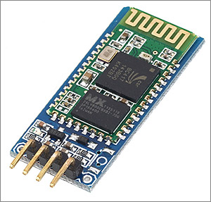
As mentioned previously I’ve decided to integrate with the very cheaply available HC-06 module that you can get from China for about Β£3. These boards only require power to be applied before they will automatically find and pair with any compatible nearby device. After they’re paired then you can send and receive data using an MCU’s UART at 9600 baud.

I’ve added a LED to my schematic that will light up when the device is paired and communication between the Android app and the firmware on the board is active.

The MCU

With the ‘easy build’ aim of this project in mind there was only ever going to be one range of MCUs in the frame for the controller and that would be Atmel’s 8-bit AVRs. They’re widely available, they come in DIP packages and thanks to the popularity of the Arduino platform there’s an army of hackers out there who know something about how to write firmware for them even if their choice of platform does mean that they may never get familiar with the instruction set or the IO registers.


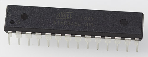
The L is important – the regular ATmega8 will not work at 3.3V

I prototyped the firmware build with the ATmega328P MCU that you can find in the Arduino Uno and when I’d more-or-less finished the code size was 12 or 13K. After moving the entire implementation from an old-style .cpp/.h structure to inline header-only methods the gcc 4.9.2 optimiser was able to really grasp the nettle and bring the image down to about 7.5Kb, and that’s with using expensive floating point operations for the PID algorithm. A round of applause from me goes to the authors of the gcc optimiser.

With only a little finishing off to do I knew I would be able to fit the whole thing into an ATmega8L. Some of the peripherals are lacking or are not as capable on the ATmega8L compared to the ATmega328P but not enough to cause me any issues.

I need to interface the MCU with some 3.3V peripherals so the actual MCU that I’ve chosen is the ATmega8L running at 3.3V and 8Mhz. As you can see from the schematic I’ve selected an external crystal with 22pF load capacitors for the system clock source even though the ATmega8L has an internal oscillator that can run at 8MHz.

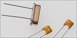
The reason for this choice is that I’ve read about considerable variation in the accuracy of the internal oscillator that could potentially affect the device’s ability to do reliable UART communications – a UART is an asynchronous peripheral that relies on each end to have accurate enough clocks to communicate. We also need it to accurately track time over a reflow program so I decided to play safe and install an external crystal.
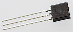
The Nokia 5110 LCD

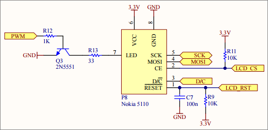
Obviously the main GUI for this project is your handheld Android device but I still decided to add a small and cheap LCD to the design to provide feedback on the current temperature and the bluetooth link status. With the addition of a rotary encoder and a button the entire process, including configuration and reflow, can be operated from this little LCD. This could be useful if you just want to do a quick reflow and don’t have your Android tablet or phone handy.

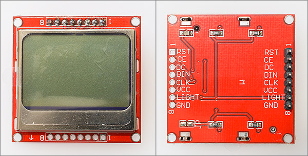
The photograph shows the actual LCD that I bought. I chose the red one because it matches the colour of the PCB that I’m using. Do note that the one that you use must have the pins in the same order on the breakout header to mine if you want it to press down directly into the board.

Another key point to note is that the backlight pin, labelled ‘LIGHT’ on the PCB must be the output from the backlight circuit and not the input. As you can see from the schematic I’m applying a PWM waveform to a transistor to set the backlight brightness in the assumption that the ‘LIGHT’ pin is an output to ground.


General purpose 2N5551 used for backlight PWM control

If you happen to get a board where the LED pin is a VCC input then my backlight circuit won’t work and you won’t have a backlight. That’s no big deal because these STN LCDs are readable in ambient light unlike the reflective TFTs that must have a backlight to allow you to see anything at all.

The fan connector


The fan will be mounted close to the triac

The fan connector will accept any 3-pin computer fan that will run at 6.3V. Most of them will do and they’ll run nice and quiet as well. My heatsink calculations indicate that I probably won’t need a fan but those calculations assume that the heatsink is in free air. When it’s enclosed in a sealed box I will have to provide some form of ventilation and may have to fit a fan as well.

Bill of materials

Here’s a table that contains the bill of materials for this project. I got nearly all the parts from Farnell and have included their part number where available for easy reference.

These parts are for a 220-240VAC design. If your mains supply is 120VAC then you’ll need to calculate appropriate substitutes. If anyone does build a 120VAC design then I’ll be happy to publish the components that are required here.

IdentifiersValueQuantityDescriptionFootprintFarnell code
ACTION, SELECT, TEMP32-Pin PCB terminal block5.04 mm(ebay)
C1, C5, C1410u3Polarized Capacitor (Radial)CAPPR2-5x111902913
C2, C622u2Polarized Capacitor (Radial)CAPPR2-5x111870976
C3470u1Polarized Capacitor (Radial)CAPPR5-8x129693602
C4100n1Panasonic ECQU2A104KLA X2 Film Capacitor1673308
C7, C8, C11, C12, C15, C16100n6Ceramic Capacitor2.54mm2309020
C9, C1722p2Ceramic Capacitor2.54mm1100369
C1010n1Ceramic Capacitor5.08mm2309024
C131u1Ceramic Capacitor5.08mm2112910
D1, D2, D3, D4, D61N400751 Amp General Purpose Rectifier2317417
D51Typical white GaAs LED5mm domed
FB1, FB2BLM18PG221SN1D2Ferrite beadAXIAL-0.32292304
JP11Header, 2-Pin, Dual row2.54mm
P11Header, 6-Pin5.08mmA18QN (maplin)
P313-Pin fan header2.54mm588581
P42Header, 4-Pin2.54mm
P61Header, 3-Pin, Dual row2.54mm
P81Nokia 5110 breakout board on 8 way female header2.54mm(ebay)
Q1, Q2, Q32N55513NPN Bipolar TransistorTO-929846751
Q4BTA12-600BWRG1Silicon Bidirectional Triode ThyristorTO-220AB1057276
R13601ResistorAXIAL-0.52329779
R2, R5, R121K3ResistorAXIAL-0.32329486
R3275VRMS1Varistor (Voltage-Sensitive Resistor)Varistor 20D series1856919
R4471ResistorAXIAL-0.31128034
R64701ResistorAXIAL-0.32329531
R7, R9, R10, R1110K4ResistorAXIAL-0.32329474
R81001ResistorAXIAL-0.32329473
R13331ResistorAXIAL-0.32329516
T16VAC1Myrra 441931689073
U1LD1117V501800mA Low-Dropout Linear Regulator, 3-pin TO-220TO-220AB1087175
U2LD1117V33C1800mA Low-Dropout Linear Regulator, 3-pin TO-220TO-220AB1703357
U3MOC3020M1Opto-TriacDIP-61471017
U418-Bit AVR Microcontroller with 8K Bytes of In-System Programmable Flash MemoryDIP-289171533
U5MAX31855KASA+1Cold-Junction-Compensated K-Thermocoupleto- Digital ConverterSOIC127P600-8AN
Y18MHz1Crystal OscillatorHC49 thru hole2063945
HS1Heatsink1Ohmite FA-T220-38E2097690
Thermocouple1K-Type thermocoupleBare wire(ebay)
Hex PCB standoffs2brass standoffs for the LCDM3 x 11mm(ebay)
HC-061Bluetooth module4-pin breakout board(ebay)
PCB jumpers22-pin PCB jumpers2.54mm (0.1")(ebay)

PCB design

I decided to go for a two layer board that fits within a 10x10cm square. This means that you can get 10 copies of the board printed at one of the Chinese online services such as Elecrow, Seeed or ITead for about US$13. I’ve been using Elecrow recently and have been very happy with their service. I uploaded my gerbers to their site, paid the fee and went and did something else for 3 weeks. Time passes…

I laid out the PCB with the high side of the board marked off at the top left. A warning legend in the silkscreen states the obvious about the high voltage present in that area. There is no absolute number for the width of a trace required to carry a given current across a PCB. Increasing the width of a trace will lower the electrical resistance and hence decrease the power loss and the heat generated to dissipate that power loss. If you approach the problem with power-loss and heat in mind then you can calculate a figure for the trace width that’ll deliver those numbers for you.

No, I’m not going to subject you to the mathematics behind it all because there are on-line calculators out there that’ll let you experiment interactively with your numbers. I settled on a trace width of 140mil which for an outer layer on 1oz copper conducting 8A would result in a 20°C worst case temperature rise for a power loss of 500mW.

The only exception to this 140mil design rule is the middle pin of the TO-220 package that houses the triac’s MT2 terminal. There’s just no way around the fact that you have to neck down the trace quite drastically to get it through the middle pin.

I’ve tried to ameliorate this by mirroring the narrow part of that trace on the bottom layer of the board and joining it to the top layer with a pair of vias on each side.

There are standards for how close high voltage traces can get to other traces (creepage distance) that take into account the environment that the product will operate in (pollution level). You might be surprised at how low those minimums are; for this board 1.5mm would be enough. I leave much more spacing than that and I also provide routed cutouts in the places where the high voltage areas come closest to low voltage.

The bottom side of the board outside the high voltage area is filled and connected to the GND net. Likewise for the top layer except the fill is connected to the 3.3V net. Having GND and VCC as fills on alternate sides takes out the two largest nets from the routing problem and makes it easy to route the rest of the board.

The four corner mounting screw holes are part of the earthing strategy and will be screwed into the metal enclosure that I use to house this project. The three screws that are in the low voltage area also connect to the GND plane on the bottom.

Building the PCB

The only surface mount device on this PCB is the MAX31855 and it has a low number of generously spaced pins. I eschewed my hot air gun, previous reflow oven and hot plate in favour of a plain old iron and the tack-soldering method because I wanted to show how easy it is to assemble this PCB and you can see me soldering the MAX31855 in the video that accompanies this article. No laughing at the back please; it’s hard to solder from behind a video camera!

Of course the remainder of the through hole components are very easy to solder, if a little time consuming due to all the bending, threading and trimming of leads. There are a few tips I can give for building this board:

  • Start with the lowest profile components and work up to the tallest. That way when you flip the board over to solder a component it should rest on itself which helps prevent it falling back through the board.
  • The pin-spacing in the footprint for the 2N5551 transistors in the TO-92 package is quite narrow. To avoid solder bridges I recommend starting each pin with a clean iron and taking care to not over-apply solder.
  • I use sockets for my ICs. You don’t have to but you’ll remove the possibility of causing damage through excess heat if you use sockets.

Important safety note

The mains traces on the top of the board may run directly under the metal of the Triac heatsink. It will depend on the type of heatsink that you have chosen to use and it definitely happens with the large Ohmite FA-T220-38E that I have selected. The solder mask is then the only thing preventing the heatsink becoming live and of course solder mask is far from being an appropriate insulator for mains voltages.

To avoid this issue, simply ensure that there is at least a couple of millimetres of air-gap between the bottom of the heatsink and the board when you solder the Triac into place. The large lugs on the bottom of the heatsink fit into the board holes provided for them and can be soldered into place to totally prevent any movement.

Alternatively, insulate the base of the heatsink with electricians tape rated well in excess of the AC peak voltage which is about 340V in the UK and 170V in the USA.


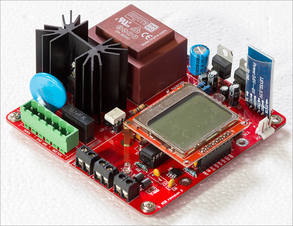
Click for a larger image

Here it is, fully built. There’s something deeply satisfying about completing a through-hole board. All the large components make it really look like you’ve actually built ‘a thing’. I know that technically you achieve a lot more for a given surface area with surface mount but the finished article does often look a bit like a few black plastic shavings with some capacitative dust sprinkled hither and thither. Old school wins in the looks department for me.

The firmware

The firmware for this device was compiled using avr-gcc 4.9.2 and can be cloned from github. You can compile it from source or you can flash it directly to the MCU if your mains frequency is 50Hz. I include a reference build for 50Hz mains supplies in the bin folder.

Flashing the program to the MCU

The firmware can be uploaded directly to the MCU using a USBASP 3.3v programmer connected to the P6 header using jumper wires. Avoid the older version of the programmer that only supports 5V programming. The newer versions have a jumper that allows you to select between 5V and 3.3V.

For safety please do not program the MCU while the board is connected to the mains. The jumpers must be removed from JP1 and a DC power source connected to pins 1 and 3. This power source connects directly into the 5V LD1117 regulator. If you have a bench power supply then 6.3V would be ideal. If you don’t then a wall-wart that can supply between 6.3 and 12V would work. Don’t attempt to use a 9V battery because they can’t supply enough current for long enough.


Jumpers on = transformed mains (as illustrated). Jumpers off = DC supply

Flashing is a two step process using the avrdude utility. Firstly you should program the MCU fuses to use an external crystal instead of the internal oscillator. The command for that is:

avrdude -c usbasp -p m8 -e -U lfuse:w:0xff:m -U hfuse:w:0xd9:m

You only ever need to program the fuses once. Secondly you should program the MCU, again using avrdude:

avrdude -c usbasp -p m8 -e -U flash:w:awreflow2.hex

That’s it. The board should now be up and running. You can of course re-run the programming command as many times as you need to.

Compiling from source

I use scons to build the firmware. To compile, cd into the atmega8l directory and use scons to build it:

$ scons
scons: Reading SConscript files ...

Usage: scons mains=<FREQUENCY> [upload]

  <FREQUENCY>: 50/60.
    50 = 50Hz mains frequency
    60 = 60Hz mains frequency

  [upload]
    specify this option to automatically upload to
    using avrdude to a USBASP connected MCU.

Examples:

  scons mains=50     // UK mains frequency
  scons mains=60     // USA mains frequency

A timer peripheral is used to work out where in the half-wave I need to turn the triac on and off. The duration of a half-cycle is different for people on 50Hz and 60Hz supplies therefore the build command needs to know which frequency you are on so that it can pass that information to the source code through a preprocessor definition.

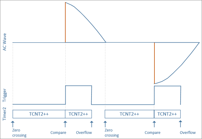
The timing part of the controller firmware is probably the most interesting. Let’s take a look in detail at how it works. The one-paragraph summary of the flow of control is this. The zero-crossing event triggers an external interrupt in the MCU. The desired power percentage is used to calculate a timer comparator value and the timer is started. The comparator triggers an interrupt and the triac gate is activated inside the interrupt handler. The timer is bumped forward so that its counter will overflow in a number of ticks equal to the triac’s gate minimum latching pulse width. When the overflow interrupt is triggered the triac gate control is released and the timer stopped. The triac will remain latched until the next zero crossing and the whole thing starts again.

This sequence allows us to control the triac asynchronously and under interrupt control. The following diagram should serve to illustrate the explanation in the previous paragraph.

I’m using the TIMER2 peripheral on the ATmega8 to do the work. TIMER2 is an 8-bit up-counter with a comparator register. It can raise an interrupt when the comparator is matched and when the timer overflows, that is it ticks over from 255 back to zero. The timer clock can be sourced from the CPU clock and has a number of divider options so that you can have the resolution that you need.

In the zero crossing handler I start the timer like this:

// OCR2 is the comparator register. See main source code for
// the code that calculates the _counter variable.

OCR2=_counter;
TCNT2=0;

// start timer at 8MHz / 1024 = 128uS per tick

TCCR2=(1 << CS20) | (1 << CS21) | (1 << CS22);

The choice of 128µS per tick is made so that the timer doesn't overflow during the 50Hz/2 half wave. When TCNT2 reaches the _counter variable the comparator interrupt will trigger, and here's the handler:

/*
 * The comparator ISR handler
 */

inline void OvenControl::timerComparatorHandler() const {

  // activate the triac gate. we must hold it active for a minimum amount
  // of time before switching it off

  GpioActivateOven::set();

  // the overflow interrupt will fire when the minimum pulse width is reached

  TCNT2=256-TRIAC_PULSE_TICKS;
} 

Now the timer is running again and will overflow after TRIAC_PULSE_TICKS clock ticks have elapsed. TRIAC_PULSE_TICKS is defined in the SConstruct build file as 4 which is 512µS and is enough to latch the BTA312 triac.

Finally, when the overflow does happen here's the handler:

/*
 * The overflow ISR handler
 */

inline void OvenControl::timerOverflowHandler() const {

  // turn off the oven

  GpioActivateOven::reset();
 
  // turn off the timer. the zero-crossing handler will restart it

  TCCR2=0;
}

A millisecond timer

I need a general purpose timer for checking timeouts and performing short delays so I use TIMER0 for that purpose. TIMER0 is the least capable of the three timers on the ATmega8L so I'm always pleased to find a use for it. Here's how I set it up:

TCCR0 |= (1 << CS01);     // CLK/8
TIMSK |= (1 << TOIE0);    // Timer0 overflow interrupt

CLK/8 gives me an 8MHz/8 = 1MHz 8-bit counter. It'll overflow every 256 ticks so the overflow interrupt call frequency will be (CLK/8)*256 = 256µS. If I were to increment my millisecond counter every 4 ticks then I'd get a counter that ticks every 256*4 = 1024µS. That's no good, I need 1000µS for an accurate counter which would mean an overflow interrupt every 250µS.

The solution is to add 6 to the TCNT0 register each overflow interrupt and this is possible because TCNT0 is read/write at all times. The overflow interrupt handler looks like this:

ISR(TIMER0_OVF_vect) {

  using namespace awreflow;

  MillisecondTimer::_subCounter++;

  if((MillisecondTimer::_subCounter & 0x3)==0)
    MillisecondTimer::_counter++;
  
  TCNT0+=6;
}

Communicating with the MAX31855

The MAX31855 is a SPI slave device implemented with 3 wires: MISO, CS and SCLK. The Nokia 5110 board on this controller is also an SPI slave device and the ATmega8L has only one SPI peripheral therefore I share the SPI bus by using different CS lines for each device. Here's the SPI pin initialisation code:

// SPI limiting values:
//   1. Max Nokia 5110 LCD clock = 4MHz
//   2. Max MAX31855 clock = 5MHz
// Selected clock is osc/4, mode is 0

SPCR=(1 << MSTR) |                  // master
     (1 << SPE) |                   // enabled
     (0 << SPR1) | (0 << SPR0);     // (for clarity) we are intentionally choosing fosc/4 here

SPSR |= (1 << SPI2X);

// clear interrupt flag by reading this register

uint8_t dummy __attribute__((unused))=SPSR;
dummy=SPDR;

Some of the firmware operates under asynchronous interrupt control and some of it works synchronously via a main loop. The SPI communication works in the main loop. I sample the temperature from the MAX31855 every 500ms like this:

inline bool TemperatureSensor::loop() {
  uint8_t i;
  uint32_t value;

  // if ready then process the raw response

  if(MillisecondTimer::hasTimedOut(_lastTemperatureTime,500)) {

    // bring CS low

    GpioSpiCs::reset();

    // clock 4 bytes from the SPI bus

    value=0;
    for(i=0;i<4;i++) {
      
      SPDR=0;                             // start "transmitting" (actually just clocking)
      while((SPSR & (1<<SPIF))==0);       // wait until transfer ends
      
      value<<=8;                          // make space for the byte
      value|=SPDR;                        // merge in the new byte
    }

    // restore CS high

    GpioSpiCs::set();       // deselect the slave

    // parse out the value/code from the packed response

    processResponse(value);
    _lastTemperatureTime=MillisecondTimer::millis();
    return true;
  }

  return false;
}

The 32-bit response from the SPI bus contains the temperature and some status information about the state of the thermocouple. The MAX31855 is able to detect states such as open circuit and shorts to GND and VCC. Here's my conversion code. I take only the integer part of the temperature, discarding the fractional part.

inline void TemperatureSensor::processResponse(uint32_t value) {

  // we need a sane compiler

  static_assert(sizeof(Response)==3,"Internal compiler fail: sizeof(Response)!=3");

  if(value & 1)
    _lastTemperature.status=Status::OC_FAULT;
  else if(value & 2)
    _lastTemperature.status=Status::SCG_FAULT;
  else if(value & 4)
    _lastTemperature.status=Status::SCV_FAULT;
  else {

    // if negative value, drop the lower 18 bits and extend sign bits

    if(value & 0x80000000)
      value=0xFFFFC000 | ((value >> 18) & 0x00003FFFF);
    else
      value >>= 18;

    // resolution is 0.25C, divide by 4 to get the integer value

    _lastTemperature.celsius=value/4;
    _lastTemperature.status=Status::OK;
  } 
}

Communicating with the HC-06 Bluetooth module

Communicating with the bluetooth module could not be simpler. The module implements a 9600 baud UART port. You don't have to worry about pairing because it'll do that automatically when it detects a compatible master device and since I'm a slave device I only need to respond to commands that I receive from the master, and receiving commands implies that I'm paired. A flashing red LED on the HC-06 board goes solid red when pairing is successful.

Setting up the USART peripheral in the ATMega8L for 9600 board communications is straightforward:

// 9600 baud: (http://wormfood.net/avrbaudcalc.php?postbitrate=9600&postclock=8&hidetables=1)

UBRRH=0;
UBRRL=51;

UCSRA=0;
UCSRB=(1 << RXEN) | (1 << TXEN);       // enable RX, TX
UCSRC=(1 << URSEL) | (1 << UCSZ1) | (1 << UCSZ0);     // 8-N-1

I set out to prove this as a synchronous implementation with the intention of moving it to an asynchronous interrupt-driven implementation if the polling frequency of the main loop caused problems with the protocol. There were no such problems, it seems that my main loop is plenty fast enough so I left as synchronous.

Checking to see if a byte has arrived in the peripheral's data register and then reading it out is a simple task:

// is something ready?

if((UCSRA & (1 << RXC))==0)
  return Command::NONE;

// move data into storage

_commandData[_commandPos]=UDR;

Likewise, when you've got some data to send it's just as simple. You just need to wait for a flag to tell you that the data register is clear then you can write to it:

for(i=0;i<5+1+dataSize;i++) {
  while(!(UCSRA & (1 << UDRE)));
  UDR=_commandData[i];
}

There are many other reusable classes in the firmware. For example there are minimal size implementations of a rotary encoder and a debounced button. There are also very small and efficient GPIO input/output classes implemented in assembly language. You can browse the firmware here on Github.

The Android App

When designing the Android app I had the aim of it working on resolutions down to 800x480 and it should work on tablets and phones alike. 800x480 was chosen as the most common resolution available today on very cheap tablets that you can pick up on ebay. Modern brand-name phones and tablets have much, much higher resolutions. My Google Nexus 10, for example, has a resolution of 2560x1600 - the same as a high-end 30" desktop monitor.

Android programming is straightforward stuff. The need to run on low-end devices means that the APIs are necessarily quite simple. If you've ever programmed C#/WPF then you'll feel at home with the XML/code combination used to create designs and implement code-behind and there are none of the complex features such as property paths and routed events that raise the learning curve for a C#/WPF beginner.


I just can't abide small monitors! (click for larger)

The Android Studio development environment is based on the IntelliJ platform which is pretty good and definitely fit for purpose. It's not as slick and professional as Visual Studio and the Android build/debug process feels slow and cobbled together from command-line tools running behind the scenes but it does work and I've never had to break out of the development flow to go fix some plumbing manually in a config file somewhere. Google have done well to make all that stuff hang together.

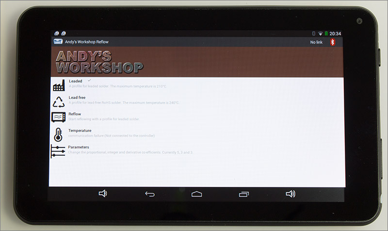
The main screen of the app lists a number of options. You can select between the two reflow profiles: leaded and unleaded. You can start the reflow session. You can see the current temperature of the oven and you can change any of the parameters that you can change using the rotary encoder input on the controller itself.

The app will automatically try to connect to the controller when it starts up and will keep trying until it succeeds. Note that communications will continue even after the user navigates away from the app. This is so that when the wife phones up to tell you to record Coronation Street while you're in the middle of a reflow session it doesn't get cancelled or suspended.

The downside of this is that you must manually close the application when you're finished to preserve your battery life. All recent android versions have a button that will show you a list of running apps. Sometimes it's a rotating list and sometimes a left-to-right list. You can use this list to close my app and save battery life.


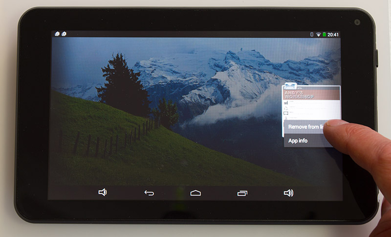
On this android version you long-press an app icon to close it

Moving on from the main screen to the reflow screen (android calls these screens 'activities') we see a reflow profile chart waiting to start. When you're ready to go you can hit the 'Go' button and the process will start.

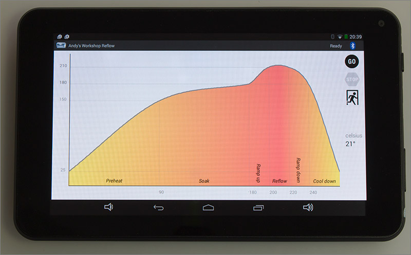
A cool glowing green blob will track the progress of the reflow session and you can see this in action in the video that I've linked in later in this article. You can abort it at any time by clicking the 'Stop' button at the top right. I've provided an 'Exit' button to go back to the main screen but you can just as well use Android's built-in 'Back' button.

Credit where credit's due, the icons used in my app are from the icons8 site.

Watch the video

I've uploaded a video to YouTube that shows me going through the build process and then doing a test run at the end. It came out surprisingly long at just under an hour so if you don't mind watching me waffling on for ages then click on the link below to watch it.

Build your own

If you're interested in building one of these boards then here's a summary of the steps you need to take.

  1. Download the gerbers from my downloads page and send off to Elecrow, ITead or Seeed to get them manufactured.
  2. Order the parts from the bill of materials from Farnell or your favourite local supplier. Build the board. The video might help you with this.
  3. Clone the firmware from Github.
  4. Upload awreflow2.hex to the ATMega8L using a USBASP 3.3V programmer connected to the board pins while powering it with 6.3V from a bench power supply. (see Flashing the program to the MCU in the main article).
  5. Enable application side-loading on your Android device then install awreflow2.apk from the bin/ firmware directory. Update! You can now get the app direct from Google Play by searching the Play Store for Andy's Workshop.
  6. Switch the controller on first, then the Android device. Pair them. The HC-06 pairing code is probably 1234. Now start the app and wait for the connection. It will take a few seconds.

Enjoy your reflow controller and remember, always treat the mains supply as potentially deadly. Never work on or even touch any part of the board while the mains supply is connected and never work on a mains project unless you're able to give it your full and undivided attention at all times.

That's all for now folks. I hope you've enjoyed reading this article and if you've got any comments then please feel free to leave them below. Questions and discussions can be posted over in the forum where I'm looking forward to hearing your thoughts.

Update 1: improving the phase angle timing

A reader contacted me to suggest that the mapping of the output from the PID algorithm (a percentage) could be improved by considering a non-linear mapping to the mains phase angle. Currently my algorithm linearly maps the desired power percentage to a time along the x-axis of the half-wave. This does not take into account the rising and falling of the waveform — particularly at the start and end of the phase.

So I started thinking. It seems logical that the actual output power at a given phase angle is going to be proportional not to the linear distance along the axis but to the area under the curve. The area under the curve is the definite integral from zero to the phase angle. I could pre-calculate a mapping table of desired output power percentage to a linear percentage phase time duration and store it in flash at a cost of just 98 bytes.


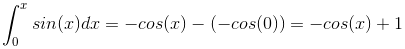
The area under the curve is an easy integration formula

I fired up Excel and got calculating. You can see the results in the spreadsheet in the doc directory on Github. Beware that this spreadsheet contains array formulae that Excel appears to be spectacularly bad at recomputing. Be ready for a few minutes of delay when you open the worksheet.


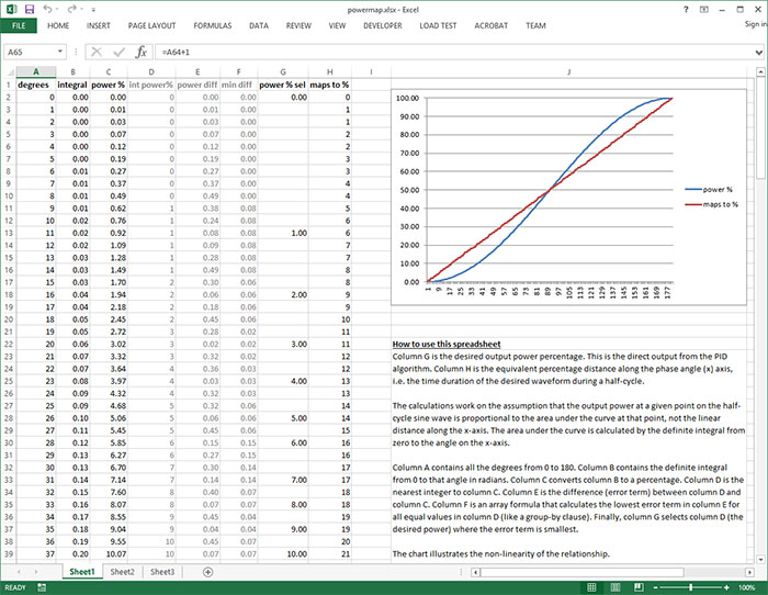
Calculating a lookup table with Excel

The output from the sheet is a mapping of the desired output power percentage to a linear integer percentage that has the least error from the ideal percentage.

The implementation in OvenControl.cpp and OvenControl.h is trivial and I moved quickly to running a test cycle.
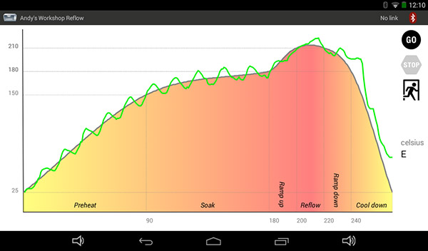
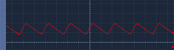

Test run results

The improvements are noticeable in the way that the oven applies power at the low and high ends of the output but I clearly have more work to do to eliminate the oscillation that I get as the algorithm struggles to accurately follow the curve. I intend to improve the insulation, tweak the algorithm parameters and increase the temperature sampling rate in the firmware and the app. More updates to follow.

Update 2: fixing bugs, addressing heat loss

I think I've finally got it where I want it now. There were a number of issues that I addressed to get to this end state.

Firstly there was a bug in the android app. It was supposed to sample the temperature at 0.33Hz on the options screen and 1Hz during a reflow job. The bug meant it always sampled at 0.33Hz. I've changed the logic to 0.5Hz for the options screen and 4Hz for the reflow job. The source and compiled binaries on github have been updated.

Secondly I've insulated the top of my oven with foil. I can't understate the difference that this has made. Heat loss through the glass top was the single biggest issue.


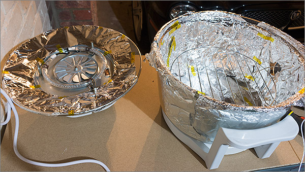
Fully insulated oven (with small observation gap in lid)

Thirdly I've changed my PID parameters to 10/1/0. A large proportional component makes the oven react quickly when needed. I don't need a derivative component.
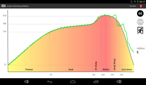
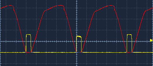

Test run

The difference is amazing — particularly the insulation. The oven never has to apply 100% power except for a second or two during the ramp-up period. The rest of the time it just gently applies small nudges to the temperature. Ignore the steep ragged falls at the end — that's me lifting the lid to cool it down because the oven has no means to actively lose heat.

You can see the effect of all these improvements in this followup video:

Update 3: Bug fixes and ATMega8L firmware improvements

Version 2 of the app is now available from the Google Play Store and fixes a few minor issues. I'd advise everyone to upgrade to this new version. Details of the bugs that were fixed are in the Play Store release notes.

There's also a new version of the ATMega8L firmware available now in github. This release fixes bugs in the manual reflow option and adds a new feature that continually shows the current oven duty cycle while the android device is connected.

Bare PCBs for sale

I've got quite a few of these blank boards left over from the batch that I received from Elecrow and I'm happy to sell them on a first-come-first-served basis.


Location


  • Pingback: Android-based Reflow Brings Solder Profiles to Your Lab | Hackaday()

  • Pingback: Android-based Reflow Brings Solder Profiles to Your Lab | Hack The Planet()

  • salman sheikh

    Where can I get the myrra in the us without paying $20 for ordering from England stock?

  • Jahn

    Thanks for your project. Nice as usual. Keep doing such projects, please.

  • Kari Argillander

    I have my own oven project, but i still decide build this one πŸ˜€ I ordered 10 pcb. If you live in Finland please contact me 0407455230 and i can send you pcb little bit cheaper.

  • Kari Argillander

    There is a mistake in part list. I do not need 7 C4 capacitor. πŸ™‚ Also bluetooth module and jumpers are missing. Do you have any case for this. I would like to get link if you do.

    • Hi, thanks for the correction, I’ve fixed the caps. The two 100n rows were merged in the exported BOM and I didn’t correctly adjust the quantities when I broke them out. The HC-06 is just one of the many on ebay. I bought item number 281539663639. The jumpers are standard 0.1″ pcb jumpers again from ebay. I haven’t made a case yet. Making enclosures is something I know nothing about so it’ll be a learning experience for me.

  • Kari Argillander

    I found couple more mistakes. In BOM there is too many regulators. Also I found that select, action and temp pins are not 2,54mm pitch. In BOM you say they are. Also identifier say’s “ACTION, P5, P2” I think it should be “ACTION, SELECT, TEMP”. Just get my PCB’s can’t wait to build this up.

    • Many thanks again Kari. I have corrected the errors. Man I made a mess of the BOM export. Hope it’s OK now.

  • JB

    Very nice work.
    I think I’m going to build this as I want some way to make better PCBs and although I had some decent sucess using hotplates to do surface mount components there was so much luck involved, sometimes it worked perfectly,. other times components weren;t soldered or the board got charred.

    Any advice on what kind of oven to get to base it one?

    Thanks for documenting this, the project is interesting but your writeups are excellent!

    • Hi JB, thanks very much for your comments they are much appreciated. I highly recommend a halogen oven. The one I use is a 12 litre 1300W generic oven that I got on ebay. Like this one. When fully insulated with foil they keep up with the reflow profile with ease. I’m so impressed that I think I’ll shoot another video soon showing it in action again.

      • JB

        Excellent and thank you.
        I intend to build one of my own. It will take me a while due to lack of spare time at the moment but I’ll get there!

        I’m more interested in the fpga / lcd side, but need a way to make PCBs that works somewhat reliably for that so I’ll experiment with that first on some simple projects

        • JB

          I’m going to make a Frankenstein combination of your two projects over the next week or two. Using bluetooth for control but a solid state relay for power control.

          I’ve got a cheap STM32F microcontroller module. I’ve already tried it with a thermocouple module and it can read the temperature and with the same serial bluetooth module and that works fine too. It seems to be able to drive a solid state relay directly just about (although I’d use a driver transistor in a real build) and I’d use that because the relay is much easier than the circuit you’ve used here (and frankly safer as I’m not 100% happy with mains power just yet).

          I’ve basically tested all of the parts individually and it all seems to work, so I just have to put it together nicely and safely and then obtain the actual oven and write or adapt software for it all. Using a bluetooth module for an interface on a phone is what makes it practical and cheap and easy so thank you for that idea.

          Once it’s built and working, I can make a custom PCB for it all much more easily πŸ˜›

  • Sam H.

    Hi Karl,

    I’m interested in building your reflow controller, if you have time could you tell me:

    What would rough cost be for a full build?
    Can I edit/produce my own profiles?
    Would there be a limit on profile values (time), i.e. extreme case, could I set soak time as long as 2 weeks?

    Thanks,

    Sam

    • Hi Sam, the BOM cost is probably less than Β£15 plus the PCBs wherever you decide to get them made. If you know your Android programming then you can edit the app code and create your own profiles.

  • Pingback: Android Based Reflow Controller - Electro-Labs.com()

  • JB

    I’m thinking of making something like this using an “arduino due” reading from a thermocouple using a prebuilt module something like this http://www.ebay.co.uk/itm/131268599779 and a bluetooth module similar to the one you used, as well as a solid state relay controlled by the arduino.

    Do you see any reason why that wouldn’t work? I just feel I could do that much more quickly and easily that a full project and then use the thing to build more interesting (to me) projects πŸ™‚

    Also, have you tried using BGA components with this at all? There is a project I’d like to use a CPLD device in but the cheapest one that suits seems to be a 64 pin BGA and I was wondering if you thought this would be good enough to reliably reflow that? (Assuming everything else is done right of course)

    • Hi JB. Yes that would work. Attaching boards together like that is exactly how I prototype things like this except I favour the STM32 for ARM development.

      • JB

        Ah yes, it would be quite difficult to lay out the traces on a cheap board.

  • Pingback: Projects i want to do. | John's Ramblings()

  • Hi Darko, yes I have spare PCBs that I can sell. The reason I didn’t
    advertise them on this page is that postage costs are quite high to send
    abroad from the UK. If you’re interested then send me a note with your
    country using my Help/Contact form and I’ll work out the cost.

  • Patrick

    Hi Andy, sorry to dig up and old thread but I’m attempting to recreate part of your project on perf-board as safely as possible. I’m hitting what I believe to be some potentially dangerous roadblocks and I don’t quite know how to safely debug it. To start, I’ve made a few changes to the design: no transformer or voltage regulation section (I provide wires for an MCU interface and power), a different zero cross circuit which I’ve already verified works, and and have adapted the driver for 120VAC U.S. mains. The TRIAC circuit is essentially the same though. The issue I’m having is that when the 3.3V TRIAC_ACTIVE signal is going to the driver, I know I’m getting about 40mA through the MOC310M emitter (tested w/ mains disconnected) but the TRIAC does not activate when the mains are connected. I’ve double checked the connections but I rarely work with high power and I don’t know a good way of testing and debugging beyond that. I’ll probably shelve this for a while and do some safety research in the meantime but I wanted to know if you had any recommendations for proceeding. Thanks

    • Hi Patrick. When I was prototyping this I used a portable lamp hooked up to the triac to provide a load that could be switched on and off. I assume you’re using a MOC3010M and have substituted a 180ohm resistor where I used a 360 and also that you’re using the same type of triac that I’m using. I don’t see any obvious problem with your testing approach – perfboard is OK for mains testing (breadboard is not) and as long as you can remotely operate the supply and can do your tests “hands off” then you should be fine. Basically I would hook everything up, stand away and plug it in at the wall, observe and then remove from the wall. Are you sure that no components have been damaged during prototyping (particularly the MOC)?

      • Patrick

        Thanks for the tips. I built a smaller, simpler circuit with the TRIAC just for a few sanity tests and managed to figure it out. I’m kicking myself for not realizing it sooner but I was operating under the assumption that because a TRIAC is bidirectional, MT1 and MT2 should be interchangeable. Not the case at all. Putting the TRIAC on the other side of the heat sink to switch the pins cleared everything up.

        • Good to hear that you got it working. If I guessed wrongly in my schematic for any of the component values that should work on a 120VAC supply then please let me know and I’ll be happy to correct them.

  • Agate Palim

    do you plan to upload the app to the google play store? this way it is easy to distribute updates. and do you think it would be possible to update the atmega-firmware via bluetooth? in this case the android app could also update the Β΅c

    • I don’t have any plans to pay the $25 access fee to the Play Store just yet, though I may do so in the future because it’s quite affordable and only a one-off fee. The Atmega firmware is very, very close to the flash limit with only about 200 bytes remaining free. A bluetooth flasher would not fit in that space.

      • Agate Palim

        Hey Andy, maybe you could make the app $0.50 for the first 100 downloads πŸ˜‰ I would definitely pay 50 cents just to support this Project! (even without the current need/space/time for a reflow oven) And about the Atmega8L: It could be replaced with an ATmega168.

        • I’m on the app store! Now anyone can download the app without having to faff around with the sideloading hack. Search ‘Andy’s Workshop’ on the Play Store or click the above link.

          • That is great Andy and will make doing your project just that little more achievable, seeing as getting that part of your project working would have been very challenging to me. Thanks a lot

  • Angelo

    Very interesting and informative project Andy! Im trying myself to build a tool for bga reflow but of course it is not an easy task., Your suggestions are of a great help.Your explanations are also very clear. Thank you again
    Angelo

    • Thanks Angelo. It would be great to see a write-up of your BGA reflow technique if you do get it working. There are not many hobbyist-friendly BGA articles out there and it’s such a painful package to work with.

  • Leonid

    Hi, somewhere you mentioned that you use ATmega328 for prototyping. Do you still have the code for ATMega328?

    • I’m afraid not. After the ATmega8L’s arrived I migrated the code and then the development moved forward only on the 8’s. Really though, as I remember it the timers were the only difference and the 8’s were more limited than the 328’s so it should be easy to back-port to the 328.

      • Leonid

        Thanks, Andy. I will try…

  • Hi Andy, great project. Is it OK to use your controller with an ordinary electric toaster oven 240v 50 hz I live in Australia. The reason I ask is because I just bought this controller but I would also love to build yours https://www.beta-estore.com/rkuk/order_product_details.html?p=242

    • Hi Peter, yes the components I used are valid for your supply (it’s the same as ours) and should work with your toaster oven. I designed the board to be safe at a maximum of 8A. Your toaster oven should not consume more current than that but do check it.

      • Thanks Andy and as I said it is a great project and thanks for sharing

  • Ed Latuta

    Hi Andy, Impressive project. I would like to try to build my own too. Do you still have some boards left?

  • Karolis Kubaitis

    Hi Andy! Thank you for sharing!!! I’ve almost built it, just waiting for thermocouple to arrive. Looks like I got a faulty 5110 lcd as it does not display anything, there is no backlight as well. Your app detects HC-06 module and under the “Temperature” tab “Waiting for a communications link” is displayed. When I’m trying to start a reflow I’m getting error message “Bluetooth data link not active”. Does it need thermocouple connected to work? Kind regards!

    • Hi Karolis. The thermocouple is not required for the app to work. It sounds like the tablet/phone is not establishing a bluetooth connection. Ensure that they are paired. Pairing happens between the phone/tablet and the HC-06 without the app or the MCU being involved. After pairing when the HC-06 is waiting for a connection its red light will flash. When the app has established a connection the red HC-06 light will go solid and the LED on the reflow board will light up. If there’s a fatal problem with the connection then the HC-06 will flash its LED slowly (you’ll know it when you see it). Sometimes it can take ~20 seconds to connect. Sometimes it’s immediate. Sometimes I have to kill and restart the app and/or power-cycle the board. Powering up the board, then starting the app seems to be the most reliable sequence. It seems the more expensive androids (e.g. Samsung) are better at connecting reliably than the cheaper no-name devices. I also think that the HC-06, being very cheap, is quite fussy about the order that things happen during the connection phase.

      • Karolis Kubaitis

        Thanks for a quick reply! Same problem occurs on both of my devices Nexus 7 and HTC One M8. Just double checked and verified that flash is correct on my cheap atmega8l from ebay. I wonder that both LCD and HC-06 are faulty.

        • No worries. Glad it works.

          • Karolis Kubaitis

            One more problem πŸ˜€ ouch, not sure but looks like my M31855K is faulty. I’ve got it from ebay and desoldered from development board. I’m getting 0 Celsius permanent reading, same results when using different thermocouples. Ordered new MAX from farnell and waiting for it to arrive. Maybe there is a way to test M31855K?

          • I’ll never buy another IC on ebay because they seem to be either all fake or QC fails. Testing is really just a case of hooking up the power and talking SPI to it.

  • Rando

    I took some time for fun yesterday, and did the simple port to AVR Studio 7.0, to provide simulation and to investigate hosting on an ATMega16a, for JTAG debug using my MK II JTAG debugger.

    Here’s a link to the downloadable project. I don’t have any way to test, but the compilation runs without error.

    Here are the relevant switches to the command line necessary to meet the stringent memory requirement to fit in 8k.

    env.Replace(CXXFLAGS=[“-mmcu=atmega8”,
    “-Os”,
    “-g”,
    “-flto”,
    “-DF_CPU=8000000”,
    “-DTRIAC_PULSE_TICKS=”+`triac_pulse_ticks`,
    “-DTICKS_PER_HALF_CYCLE=”+`ticks_per_half_cycle`,
    “-DMARGIN_TICKS=”+`margin_ticks`,
    “-DF_CPU=8000000”,
    “-std=c++11”,
    “-Wall”,
    “-Werror”,
    “-Wextra”,
    “-pedantic-errors”,
    “-fno-rtti”,
    “-ffunction-sections”,
    “-fdata-sections”,
    “-fno-exceptions”])

    env.Replace(LINKFLAGS=[“-Wl,-Map,awreflow2.map”,
    “-mrelax”,
    “-g”,
    “-flto”,
    “-Wl,–gc-sections”,
    “-mmcu=atmega8”])

    https://drive.google.com/file/d/0B75yepgXDk6rYm03aEhDQ1ZyX00/view?usp=sharing

    Need to check on if the clock speed and other MACROS are set correctly.

    Best,

    R.

  • Jonathan Williams

    Could you just crack open the oven and switch the fan and lamp seperately? That’d help you vent heat better.

  • Dino Solomon

    Hello Mr Brown.
    I ordered PCB from ELECROW for this project
    Uploaded your gerber files to Elecrow and complete an order.
    A big surprise after 3 weeks waiting. The GND layout on top and bottom missing.
    I am only a hobbyist and do not understand how the Cu layer can by separate and print only signals traces
    Have you send to them a early version and they used the negative for my order ?
    I only looking for more info to understand what happen.
    Thank
    Dino

    • Dino, IMHO I would be the gerber files into a gerber viewer and checking that those ground planes are showing in the relevant layers. If they are one might assume that the board fabricator has made a mistake with your job.

    • Assuming that the Gerbers were unmodified then it looks like Elecrow’s board house have messed up the manufacturing and I would ask them to rerun the order for no charge. I have never seen this before and I’m finding it hard to see how the board house could do this without manually modifying the GTL and GBL files. To verify, I downloaded my own upload and checked it again in Viewplot 1.5. I always check every Gerber in Viewplot as a final step before sending for manufacturing. Here’s a small screenshot of the GTL, GTS and GTO layers with GTL on top so you can see what Elecrow received from you.

      Please keep me informed as to what their explanation is because I’ve never seen this happen before.

  • Pingback: Homemade Reflow Controller with Android & Bluetooth via @andyworkshop « Adafruit Industries – Makers, hackers, artists, designers and engineers!()

  • Avirut Thi

    Hi Andy, thank you for your support.
    I have some problem ,
    1.I connected HC-06 with Android that Paring success red HC-06 light go solid but the LED on the reflow board not light up.
    2.Connected HC-06 with LCD that show “No-link” , How to solv this case ? and concern hardware in board or not ?

    • If you have a solid red light but no link then it is likely that the app is blocked somewhere in this code. If you can debug the app in Android Studio you’ll be able to tell for sure whether the connect is failing or the write/read that happens afterwards.

      Maybe your tablet/phone cannot communicate with the HC-06 after pairing? try a different tablet/phone.

      Maybe the TX/RX lines from the HC-06 to the MCU are not connected? Check board continuity and if you can spy on the lines with a logic analyser you’ll see if there’s any activity.

      Maybe the Atmega8L firmware was not flashed and fused correctly? Check your flashing and fuse setting procedure.

      • Avirut Thi

        Hi Andy, :)) Thank you very very for your guideline.
        I use “MiniPro Programmer” for flashing firmware(awreflow2.hex). And debug is fuse-bit incorrectly ,I’m setting with Atmega8L datasheet.
        Such as 8MHz external crystal /ceramic capacitor 22pF ,CKSEL0, CKSEL1, CKSEL2, CKSEL3,SUT0 and SUT1
        Now .The board can running , Thank you so much.

        • Looks like you’re all set now. I notice that you are using a toaster oven instead of halogen. Are you able to stay close to the correct reflow profile with that type of oven? I always thought that the temperature increase would be too slow with one of those ovens.

  • Gordon Brindle

    Hi, I’m in the process of building your design for the reflow controller, which I must say is extremely well documented and described by yourself. I need to wire in the rotatory encoder but I’m not too sure how it connects to the PCB connectors. ie. which wires from the encoder goes to where on the PCB. I would be very grateful if you could tell me how the encoder is connected. When I have it completed and up and running I’ll post photos so you can see it. Thank you.

    • Gordon Brindle

      Hi, I’ve now solved this wiring problem. Referring to the video where you demonstrate the construction and testing of the board: Viewing the rotary encoder from the top with the three pin side to your left, the top left pin (RED wire) is ENCB; the middle left pin (GREEN wire) is GND; and the bottom left pin (YELLOW wire) is ENCA. The top right pin (second GREEN wire) is ACTION and the bottom right pin (second YELLOW) is GND.

      • Gordon Brindle
      • Hi Gordon, glad you solved it so quickly before I even got to reply to you. I should have made it more clear with some silkscreen on the board. I might make a few tweaks in a new version soon. I’d like to re-arrange the pins on the ISP header so that they’re in the correct position to directly accept the USBASP programmer cable and I’d like to include a transformer footprint that users from the USA could use.

        • Gordon Brindle

          Hi Andy, Many thanks for your prompt reply. I haven’t started as yet to populate a PCB to your current design as I have a number of steps to perform before hand, such as calibrating my soldering iron and waiting for some additional items such as flux and Kapton tape. I’ve already programmed the MCU “off-board” so the isp header isn’t a big problem for me. I’ve created my own design for a case; I created a 3D view of it in openSCAD and created projections of the six sides which I imported into Inkscape. I’ve just sent the design of to the laser cutter lab for laser cutting; it should take up to three weeks to get back. I hope to share photos of the progress I’m making as I go along together with my design for the enclosure, too.

          I’ve attached a preview of my case looking down from the top. I took your advice and swapped around the mains input and the output to the oven. https://uploads.disquscdn.com/images/9ffe79f3afb4386a82f4fabdaf947a3ff3561dc1fe053fa515dfee38c6e29f98.png

          Best wishes, Gordon.

          • DMZ

            Hi Andy, this is amazing!
            I want to automate a kiln and have been looking for a control solution.
            I think your controller would be a real close starting point.
            I would need to bump the triac up to a 30 or 40 amp as the small kiln I found is 20 amp 120 volt. I think the bta40-600bwrg would work.
            I would mount it on a heat sink separate from the pcb board and run the “mains” power through it and not through the pc board.
            The other change would be in the “reflow profile”.
            I read earlier that you were not going to add “programability” or custom profile capability to your app. Any thoughts on adding programability?
            Either way this was fun to read through. Thanks.

          • Hi, good plan to move the mains off the board if you’re going to be running up to 40A though it. A quick play with an online trace width calculator shows that you’d need a 50mm trace width in 1oz copper!

            I am still considering the custom profile ability in the Android app. It wouldn’t be hard to do, I just need to find the time to do it.

          • DMZ

            Thanks for the follow up.
            I understand the lack of time, since i retired i have no time to do all the things i think of.
            I was looking though your computer files for the android app and came across the 2 java profiles.
            I could modify the time and temperatures, but I don’t understand the long table. Are the tables of the expected temperature for each second? If so, where did these values come from?
            I want to run the Kiln at different temperatures from about 1500 Fahrenheit to as much as 2100. I also want to run for upwards of 10 hours.
            Would this be possible if I could edit the profile files?
            Thanks again.

          • Hi, yes the long table is the expected temperature for each second. The app offers two ways to track the profile, linearly or by the smooth bezier curve. If linear then the app uses the values in the ‘ReflowRegion’ array to plot a linear route between each entry in the array. If by curve then the per-second values in the double array are used. I used Excel with a spline-curve macro to calculate the values. I’ve just added that worksheet to github. Look in the docs directory for ‘profiles.xlsm’.

            Yes you’ll be able to run your kiln at those temperatures for as many hours as you want by editing those files. Perhaps your biggest challenge will be maintaining a reliable bluetooth link for so long. I’d have to check the code to remind myself of the behaviour when the connection is lost. As I recall it will repeatedly try to reconnect.

          • Tihomir Benko

            Hi DMZ,

            Is there any success with changing the profile? I’m also interested in the possibility of changing the profile. My daughter works with a figurine of FIMO mass that is also baked in the oven, but at 110 degrees.

            Best Regards.

            Tih.

          • A ‘bake’ option is on my back burner of things to do. I would probably upgrade the controller to a 328p at the same time as well to get the extra flash space that I’d need. I wouldn’t want to do a bake option just over bluetooth from the app because you’d need to stay connected for the duration which could be hours.

          • Tihomir Benko

            Hi Andy,

            first, I would like to say: “This is amazing project!!!!”. I already built this controller and it works very well. Yes I have some trouble with HC-06 (only one of three works) and, of course, with MAX chip. But now it works. I put it in the box and tested it with the help of the bulb instead of a heater. It works exactly as specified, the light bulb strength corresponds to the percentage of the PWM displayed on the bluetooth device. Fantastic.

            I would like to publish an article about it in the magazine “Majstor” in Croatia. Is it allowed? I will definitely write who the author is and gave a link to your web site. The magazine’s edition is 10.000 copies, and readers are mostly older people.

            Best Regards!
            Tihomir Benko

          • Hi Tihomir, thanks for your comments. Good to hear that you’ve got everything working! Yes of course you can publish an article in the magazine. No problem at all.

          • Tihomir Benko
          • Tihomir Benko

            Hi Andy again,

            I would like to offer you assistance with drawing a printed circuit board for ATmega328. If you need help I will be able to work on the computer after recovery. Tomorrow I’m going to eye surgery – cataract. So, I don’t know when…

            Best Regards!

            Tihomir

  • Gordon Brindle

    https://uploads.disquscdn.com/images/2ac4f6fa2cd024ffc402b91eacd0b2692708d9bf12cceb10ba6f2ab041e0d7d8.jpg
    I’ve now finished my design for the case for my reflow controller. The box consists of six pieces of acrylic 5mm think. I used Razorlabs here in the UK to cut out my design. The box is held together by four brass pillars (60mm in height) at each of the four inner corners of the box. I decided to position the rotary controller on the back wall and use two banana type sockets for connecting the theromocouple. If I were to do the design again I would position the PCB slightly further back in the box to give more space for the connecting wires from the mains input and output.

    • John Pateman

      Hi Andy

      Thank you for documenting this fantastic build. I have just ordered the boards and components have all arrived from Farnell. I am planning on using a Daewoo oven which I came by very cheaply. I hope you don’t mind but I had a couple of questions;

      The oven I am using is quite small (10L) but out of the box only 800W. I intend to insulate it with reflective gold on the inside and an inner layer of ceramic wool and outer layer of automotive fibreglass heat mat on the outside (both good for over 300ΒΊC). I am also planning to add a pair of 200W 110V tubular mould heater elements wired in series to boost the power and mount these on standoffs from the base one in front and one behind the main element. By wiring this pair in parallel to the existing elements (and swapping the top 350W element for the bottom 450W element) I should end up with 450W at the top and 750W underneath – a total of 1200W which should be OK with the triac (at 5A). Is this a reasonable plan or do you think that the behaviour of the mixed element types will be too difficult to model with the PID? I might fit the elements and see if I can get away without using them – it will be easier to fit them now than have to come back later!

      I was also thinking about the cooling phase, which seems a bit less controlled. In my situation I was intending to open the oven door to cool down. As it happens, I have an ideal place on my oven to mount a mini linear actuator which, with a 60mm or so throw, could open the oven in a controlled manner. I was wondering if I picked up the output from Pin 6 or 26 which seem to be NC I could add a bit of code at the end of the reflow sequence to drive this pin and hence my actuator?. I could probably cobble something together using an arduino nano and a stepper driver in order to accomplish the actual movement itself but am a bit lost as far as setting this up in your code. I would need to ensure the door was closed at startup and open at the end of reflow. Do you think this is feasible? I was not suggesting that the speed of opening need be controlled w.r.t the temperature just to start an open door sequence. It would not be difficult to adjust the actual opening rate using the nano once triggered. I presume there is enough memory left to drive a single pin like this? Even if it did not drive an opener, it could be used to indicate the end of the cycle with an LED.

      Thanks!

    • Hi Gordon. I think your case looks great. Your decision to use long metal pillars for the fastenings really help the edges to look more tidy than the T-joints that I used.

  • John Pateman

    Hi Andy

    Thank you for documenting this fantastic build. I have just ordered the boards and components have all arrived from Farnell. I am planning on using a Daewoo oven which I came by very cheaply. I hope you don’t mind but I had a couple of questions;

    The oven I am using is quite small (10L) but out of the box only 800W. I intend to insulate it with reflective gold on the inside and an inner layer of ceramic wool and outer layer of automotive fibreglass heat mat on the outside (both good for over 300ΒΊC). I am also planning to add a pair of 200W 110V tubular mould heater elements wired in series to boost the power and mount these on standoffs from the base one in front and one behind the main element. By wiring this pair in parallel to the existing elements (and swapping the top 350W element for the bottom 450W element) I should end up with 450W at the top and 750W underneath – a total of 1200W which should be OK with the triac (at 5A). Is this a reasonable plan or do you think that the behaviour of the mixed element types will be too difficult to model with the PID? I might fit the elements and see if I can get away without using them – it will be easier to fit them now than have to come back later!

    I was also thinking about the cooling phase, which seems a bit less controlled. In my situation I was intending to open the oven door to cool down. As it happens, I have an ideal place on my oven to mount a mini linear actuator which, with a 60mm or so throw, could open the oven in a controlled manner. I was wondering if I picked up the output from Pin 6 or 26 which seem to be NC I could add a bit of code at the end of the reflow sequence to drive this pin and hence my actuator?. I could probably cobble something together using an arduino nano and a stepper driver in order to accomplish the actual movement itself but am a bit lost as far as setting this up in your code. I would need to ensure the door was closed at startup and open at the end of reflow. Do you think this is feasible? I was not suggesting that the speed of opening need be controlled w.r.t the temperature just to start an open door sequence. It would not be difficult to adjust the actual opening rate using the nano once triggered. I presume there is enough memory left to drive a single pin like this? Even if it did not drive an opener, it could be used to indicate the end of the cycle with an LED.

    Thanks!

    • Hi John. Does your oven have a fan? If so then any temperature gradients caused by the different size of elements will be evened out. It’ll be interesting to see how the PID algorithm performs with yours because its not halogen and will overshoot more because your elements emit heat for longer after being switched off. Still, that’s what PID is supposed to learn and compensate for but your P-I-D co-efficients will not be the same as mine. In short, you’ll be fine I think.

      With regards to cooling. If I were you I’d just open the door manually and maybe direct a fan from the outside into the open oven. When it comes to the point where cool down is required you need to do it rather quickly to keep up with the profile but the important thing, to avoid damaging silicon, is to never exceed a component manufacturer’s “max time above X degrees C” rule that they give in their application notes (e.g this one on page 21 from ST).

      • John Pateman

        Hi Andy
        Thanks for the helpful advice. I will see how it pans out when I get it running. Running into a couple of issues at the moment – flashing the Atmega – which I am sure I will sort out as I have done this several times previously. The other problem is the board design. This is really hard to solder with a fine tip iron as there is no thermal relief on the ground plane connections. I am having lots of problems with dry joints πŸ™ – so much so that I might even have to redo the schematic in Kicad and get some more boards made. Don’t suppose you have any advice on addressing this?

        BW

        John

        • Hi John, I use a 2mm chisel tip with the temperature control on my Tenma iron set to 340C. I use leaded solder with a flux core. I didn’t have any problems creating good joints with this setup.

          • John Pateman

            Thanks for that – I managed to find an old reel of leaded solder and with the temperature a bit higher I managed to solder this with my pointed tip. Forgot how much more forgiving lead is – ROHS has a lot to answer for! Now for the programming!

      • John Pateman

        Hi Andy

        OK, so all up and running! Very much like the interface and works well. I am having some issues with PID tuning – unfortunately, with quartz elements, as you predicted, there is quite a lot of inertia – the preheat has a significant lag and I seem to be limited to a ramp up rate at lower temperatures of 1.5ΒΊC /s and just about keeps up to 2ΒΊC at ramp up. Whilst I am getting good (although slightly delayed) control for the preheat, by halfway through the preheat and all the way through the soak phase I am bang on the temperature. However, I am getting into problems at ramp up / reflow as I am getting a delay and significant overshoot in the reflow region. I have been trying a variety of P values, keeping I & D terms zero. I have tried increasing the P value with the intent of finding where it becomes unstable but that doesn’t seem to happen as the profiles shapes don’t allow steady state analysis.

        Can I make a software suggestion? Would it be possible to have an extra option of a simple ‘Set temperature’ mode – this would be really useful – firstly i would like to be able to use this for a variety of controlled heating/warming operations – e.g., drying silica gel, warming moulds, curing paint, warming plastic for vacuum forming. Secondly, it would make PID tuning a lot easier! If you could change the PID parameters in a steady state situation, I think it would be a lot easier to get optimal PID values. Most of the articles I have read on PID tuning suggest trying to establish these values in a steady state model. I am not a programmer and although I have looked at the code, I am unsure how to implement this. What i would invisage is an extra option – ‘Target temperature mode’ and an adjustable temperature – adjustable via the encoder / app.

        Would you consider this extra option worth implementing?

      • John Pateman

        Pretty pleased with the profile up right up until reflow when it all goes a bit Pete Tong πŸ™ . Unfortunately I think there is too much thermal inertia from the cal rods and IR elements to ramp sufficiently fast without overshooting. Am going to try a thin aluminium tray and possibly change the elements for quartz halogen.

        I will also try backing off the P and adding a bit of I to the mix to see if that helps.

        Would still like a hook into a trigger to ‘open door’ as adding lots of insulation also mean that cool down is slow… And an auto opener is cool!

        https://uploads.disquscdn.com/images/3c7e37709533d7ce6096d1f0f0e13d7ac9ceee49478b083993f72af5a856838d.jpg

        • John Pateman

          FYI Update!

          I spent some time tweaking the PID parameters and with an aggressive differential component and a bit of I things were pretty reasonable but I still wasn’t completely happy so I went for a rebuild using a 1200W circular quartz element in the bottom and two 200W cal rods at the top of my pizza oven. I have insulated the enclosure inside with high temp gold foil and on the outside with some ceramic wool and heat reflective blanket. I have mounted the controller within the enclosure (so it is all self contained) and cut ventilation channels to ensure a good airflow over the heatsink. Cut out a front panel on my cheap Chinese CNC.

          Pretty good result, I think. The profile all the way to reflow is very accurate. There is more of a problem with ramp down/cool down as there is no active cooling other than me carefully opening the door at a carefully judged moment :).

          https://uploads.disquscdn.com/images/803bafb1cb704db692c41c7a1e4a7aedcd81a59d3d213dda4b4bfc1d3f009cca.jpg https://uploads.disquscdn.com/images/949cebf47bdef4958cb0f5233120268fcec228e4a4a2a56c7bbda02375393ee8.jpg https://uploads.disquscdn.com/images/b5419d79ca7d8308f4636a68f71c95b7d59ca6791a32ff7f4ae6c84c5b96ba10.jpg https://uploads.disquscdn.com/images/ceda431ee308eb8f7709facd9f1023224e5dababc85ecaa8b1c3c631e780ec2a.png

          • Looks great John, better even than I’ve achieved and extremely accurate. I don’t worry much about the cooling although I do treat as a bit of a challenge to see how close I can get to the curve by the time and amount that I lift the lid. Normally I end up with a curve looking like yours.

          • John Pateman

            Thank you! It has been a fun build with a few minor bumps in the road πŸ™‚ but challenges add to the fun! The ramp down and cool down phases are uncontrolled as you say but it is probably less important than the first part of the profile and the joints look good under a microscope.
            I wanted to build an oven that was self contained, front loading and had a good board size capacity and this ticks all the boxes.
            I have a some spare boards available (I am keeping one back in case of disaster ) but I have three that I am happy to sell for a modest cost + p&p.

            Learning points for me:

            The original quartz rods were fairly fast at heating up but never got ramp up speeds of more than about 1.5ΒΊC/s and there was always a bit of a lag on preheat – probably not significant in practice but I wanted to go for a tight profile. Adding in more heaters (‘cal rods’ for sold for heating moulds) helped a bit but they had significant thermal inertia too. The ring quartz element below (1200W) and the cal rods (2x 200W 110V wired in series) above give a good profile and reduces the problems of dark components overheating. I have put the board on a thin aluminium shelf which helps to distribute the heat. I initially tried a perforated aluminium plate (10mm holes and 2mm thick) over the whole bottom element as a way to distribute the heat but this nearly resulted in a fire… I will probably remove some of the bars on the grille rack to ensure there is no wicking away of heat from the underside of the aluminium.

            As you have identified, ramp up performance is improved enormously with good insulation. I used heatproof gold tape that is sold for moding hotrod exhaust pipes. It needs to be good quality and you need to clean the oven really well with isopropyl alcohol to ensure it sticks properly. Between the oven shell and the outer carcass I put a layer of high temp ceramic blanket – especially important when insulating the area where i mounted the board.

            On the flip side, more insulation means, obviously, that he cool down is slower but this is probably less of an issue.

            The programming header (as other users have found) is not a standard header pinout and ensuring a good connection for programming using multiple wires is a bit flaky. I found it much easier to program using a stand alone programmer with a zif socket.

            Desirable extras for V2 πŸ™‚
            Would be very handy to have a fixed temperature mode. I this would be helpful on two counts. It would make PID tuning MUCH easier as you could improve tuning parameters by increasing the P component until you get oscillation, then add in some ‘D’ and finally some ‘I’ (if necessary). Having a fixed temperature oven would be quite handy for all sorts of other workshop / lab tasks too.

  • BlacknWhiteWDK

    Hi Andy, I need help!
    I tried to program the Atmega as you suggested with a USBasp programmer on 3.3V and while powering the board with 6.3V, but it does not work πŸ™

    I connected the board like this:

    programmer ——- board
    VCC —— VCC
    GND —— GND
    MISO —— MISO
    MOSI —— MOSI
    SCK ——- SCK
    RST —— RST

    When I try to upload your hex or set the fuse bits with avrdude, I get the following error:
    https://uploads.disquscdn.com/images/d2a92c4fd0bfb34f10e600e9c98b11bb2a6203010b8fffdc5092031233057bb4.png

    I really don’t know what to do. I came this far with my modest hobby electronic skills, but now I’m just lost.

    • BlacknWhiteWDK
    • First we need to establish that your usbasp programmer and USB device driver are working fine. Can you successfully use the usbasp to upload a test file, e.g. a simple ‘blinky’ example to an Arduino board? If you can do that then we know that your programmer and USB device driver are OK.

      • BlacknWhiteWDK

        Thanks for your fast answer!

        Yes, I just used the usbasp successfully to upload the blink sketch to an arduino pro mini.

        • Good news. Please double-check your jumper wiring for the usbasp to the reflow board. You have to use jumper wires because unfortunately I did not arrange the ISP header pinout to the same as the cable that comes with usbasp. Also please review your JP1 setting as per the instructions under the heading “Flashing the program to the MCU” in the article.

          • BlacknWhiteWDK

            Hi Andy,

            unfortunately I already checked the wiring many times, because I seem to have some sort of a weird usbasp programmer cable.
            As far as I understand, this is the normal pinout (tiny lid on the middle-left):
            https://uploads.disquscdn.com/images/8654dff10b119e6fb3c800cb75ac5fcec04c026f03f0eb2735c3a92a9fc0dc13.png

            However, if I hold my programming cable the same way (so that the tiny lid is on the left), this seems to be my pinout:
            1 – MOSI
            2- VCC
            3 – NC
            4 – GND
            5 – RST
            6 – GND
            7 – SCK
            8 – GND
            9 – MISO
            10 – GND

            Here’s a pic of my cable:
            https://uploads.disquscdn.com/images/f1579596f77271fe4e0556fdc06bfd442162259e46961a891458a70c84ffec19.jpg

            But even if I try to connect the jumper wires according to either of the 2 possible pinouts (the pinout it should be and the pinout which I think is correct on my weird cable), it doesn’t work. Maybe I damaged the Atmega8 in the process?

          • Your Pin number labeling appears to be wrong from what I can see. This is an image I made for a quadcopter flight control board project that also uses a USBasp programmer which may clarify the situation. https://uploads.disquscdn.com/images/b6bcef35ede419eca693d8ea8755787992890b47b5aa1d7ca1faadcfbb45447c.jpg

          • BlacknWhiteWDK

            Hi Peter,

            I just tried again according to your pinout description without success. This time I connected the board directly to the specific pins on the usbasp, without using the flat cable. Still without success. Maybe there’s something wrong with my Atmega8l?
            I mean I could successfully load a sketch to an arduino pro mini with the usbasp, but programming the reflow board isn’t working (I checked the wiring so often that I am sure I have the correct wiring)

            I remember that during my numerous tests today I could successfully run the first command to program the mcu fuses to use the external crystal (
            avrdude -c usbasp -p m8 -e -U lfuse:w:0xff:m -U hfuse:w:0xd9:m) – however after that I couldn’t flash the firmware (I got the error in my screenshot above) – so I thought there was something wrong with the wiring and tried every possible wiring combination I could find on the internet, but with none of these combinations I could flash the firmware or program the fuses again (none of the two commands are working anymore)

          • Sorry that didn’t help but maybe Andy has some other suggestions. Good luck

          • It’s certainly possible to ‘brick’ an ATmega by flashing incorrect fuse values to it. Did you ever flash any fuse values except for the correct ones that you quote?

            Try removing the ATMega8L from the board and attaching to a breadboard with the crystal and its capacitors as well as 3.3V, ground, the usbasp pins (including reset). You’ll also need a pullup resistor in the order of 10k from the reset pin to 3.3V. That’s really all you need to program it ‘out of circuit’ and should help you determine if it’s been bricked with incorrect fuse settings.

          • BlacknWhiteWDK

            Hi Andy,

            no I didn’t flash any other fuse values.
            Since I have no crystal with 8mhz lying around, I just ordered a new one plus a new atmega8l. I will report back how programming goes if I use the “breadboard method”, both for the “old” atmega8l which is currently plugged into the board and the “new” one.
            Thanks for your help so far!

          • BlacknWhiteWDK

            Hi Andy,

            so I just found the problem: The female headers, which I soldered onto the board for easy placing & removing the Atmega8L apparently don’t make a full connection to every pin of the atmega. However when I connect the board and the atmega with jumper wires like in the following picture, it works!

            https://uploads.disquscdn.com/images/e559f9d4b9414d2f9797aafa105146c9d45d9bb4cdc59c305dd4fae02e3ecf77.jpg

            But now I don’t know how i can “tighten” the female pin headers so the atmega fits properly. Desoldering the female pinheaders and soldering new ones which are tighter would be really difficult, since I have no hotair desoldering station or something like that.

            Unfortunately, a new problem came up :/
            The display as well as the android app show a temperature reading of 0Β°C. Do you know why this could be the case?
            I tried wiring my thermocouple “both ways” round, but everytime I get a reading of 0Β°C. I checked the solder joints of the MAX31855, but there seem to be no bridges or something like that.

          • Hi Peter, I agree with you. Your pinout image matches mine exactly.

  • BlacknWhiteWDK

    Hi Andy, I finally managed to solve every problem I had before, however there is one more thing which isn’t working: When I start the reflow process nothing happens. I measured with a multimeter, but there is zero voltage across the two wires running to my reflow oven.

    I suppose the problem is either the TRIAC I’m using (BTA12-600BWRG) or the optocoupler (the same one you are using) – how can I troubleshoot these parts correctly? Are there other components which could be responsible?

    Thank you!

  • BlacknWhiteWDK
    • Looks nice. It does the job of keeping fingers out of harms way.

      • Martin

        Hi Andy. I really like your design and wish to have a go a building it..so I was wondering if you had any pcbs’ left or if I could buy 1 from someone in the forum? Or would there be much modification needed in code
        to use an arduino uno and ssr instead.. ? Thank you for making your work available..

        • Hi Martin, sorry no PCBs left. I sold off all the surplus boards within days of this article. There’s no technical reason why an Arduino with an SSR can’t be used but I can’t really guess accurately at the modifications that would be required other than to say that yes, extensive modifications would be required to the firmware but probably none at all to the Android part.

          • Martin

            Thanks Andy. Unfortunately I can’t code πŸ™ so I think I’ll stick with your project instead πŸ™‚

          • Martin

            Hi Andy. I managed to build your project finally, but just a couple of things to mention. I originally
            had an issue with the Bluetooth connection but got it working, my module was displaying Linvor in bluetooth discovery but when I renamed it to HC-06 it worked..Last issue I have is the lcd display backlight reverts back to 0 or off , after power is disconnected? Other settings are retained ok?
            Still having a play with my oven which i think I need to do some work on..Thanks again for your project.

  • HI,
    your using this Varistor (http://uk.farnell.com/multicomp/mcv431k20ds/varistor-710-20mm-disc/dp/1898547) in your build. I couldn’t find a place that has them in stock so I bought this one (http://uk.farnell.com/bourns/mov-20d431ktr/varistor-metal-oxide-430v-20mm/dp/2250980). This one should work right?

    • Yes, with 275VAC continuous operating voltage that one looks fine.

  • Hi, we build the thing at our space and everything went fine. We don’t have the USB programmer you have. We tried to use a AVR dragon. Sadly it didn’t work. It gave us an error when we tried to flash it.
    One of our members took the chip home and flashed it using high voltage parallel programming with his dragon and that seemed to work, but when we put the atmega back in the board it still didn’t do anything.
    We hooked up a bus pirate to it to check if their is anything on the bluetooth port but nothing.

    Do you have any idea what we could have done wrong? We checked components several times. They are all correct. Clock is running, reset is held high, power is good.

    The errors we get when we try to flash it are:

    $ avrdude -P usb -c dragon_isp -p m8 -e -U flash:w:awreflow2.hex
    avrdude: jtagmkII_setparm(): bad response to set parameter command: RSP_FAILED
    avrdude: jtagmkII_getsync(): ISP activation failed, trying debugWire
    avrdude: jtagmkII_setparm(): bad response to set parameter command: RSP_DEBUGWIRE_SYNC_FAILED
    avrdude: failed to sync with the AVR Dragon in ISP mode

    avrdude done. Thank you.

    $ avrdude -P usb -c dragon_isp -p m8 -e -U flash:w:awreflow2.hex
    avrdude: jtagmkII_getsync(): sign-on command: status -1
    avrdude: jtagmkII_getsync(): sign-on command: status -1
    avrdude: jtagmkII_getsync(): sign-on command: status -1

    • I’m afraid I can’t comment on correct usage of the ‘dragon’ because I’ve never used one. When you did manage to flash the firmware did you remember to also flash the fuses?

  • CP

    Hi !
    I’ve recently discovered your project and it’s amazing !

    But I got some problems with the triac : the BTA312 is now obsolete, what triac can I take to replace it safely ?

    Thanks !

    • The ST Micro BTA12-600BWRG is directly equivalent and can be used as a replacement. I have updated the Bill of Materials table accordingly.

      • CP

        Ok, got rid of my issue, the oven is working perfectly now πŸ™‚
        It was a solder joints that wasn’t good on Q2, and so the zero-crossing detection wasn’t working…

        Thanks for your amazing job ! You saved me a lot of time and money !

  • ava1211

    Wow, nice work. I’ve just started doing SMD work myself (after many years of through hole only) using a heat gun.

    I’ve got a ceramic (or quartz – not sure how to tell) 1600W toaster myself, any idea what sort of issues I might hit trying to apply your design to elements of this type?

    • Hi, without any modifications it would probably not respond quickly enough to follow the reflow profile. Insulation would definitely be required. After that it’ll be down to experimentation to see how well it performs. By far the best toaster-oven modification I’ve seen is this one: http://andybrown.me.uk/forum/index.php/topic,60.30.html. Click on the YouTube link in the forum post.

      • ava1211

        Thanks for getting back to me.My initial testing at low temperature (my thermometer only does 150 degrees) shows that it can do 100-130 (ramp-up equivilent) in approx 25-30 seconds (testing with a slight gap in the door for probe, filled with foil). I’m hoping with some proper wood fire oven insulation I have on order that I have enough power to do it in 20.

        On the plus side It’s quite easy to rig a small solenoid for some active cooling on this model.

  • ElektroQuark

    Hi Andy,

    I have published my version of your controller in Youtube.
    I have make a couple simple changes when assembling it.
    It could be of interest for anyone building one the 3D printed case I used.

    Take a look:
    https://www.youtube.com/watch?v=bk86r1qcdow

    Thank you very much for sharing your projects.

  • Gordon Brindle

    Hi Andy,
    I have final finished assembling my reflow controller following your instructions and to your design. I have programmed the atmega8L with your firmware using scons (although I had to use the -B 5 option with my programmer) and switched on the controller with the thermocouple attached. The display works; the rotary encoder functions in that I can select different menu options and the action button works okay in that I can select items from the menu, eg set the display contrast and brightness. The HC-06 is detected by my phone and I get a solid red led on the HC-06. I have verified that the voltages on the board are correct: 5V and 3.3V and the LED to indicate a link with your android app can be swtiched on and off okay (performed in a separate test). In a separate test I verified the thermocouple device (MAX) and it displayed room temperature and the temperature would increase if I warmed the tip of the thermocouple with my hand. The separate testing was done using an atmega328p. Also, the fan is powered on okay and runs very quietly so you chose a good fan for the project!

    Now to my problems:

    1) With the atmega8L programmed and inserted on power up of the controller the display reads “Listening”, “No link” and zero degrees C. I can adjust the temperature offset satisfactorily up and down. The display however does not indicate room temperature and does not respond to an increase in temperature when warmed by my hand.
    2) Although I get a solid link on the HC-06 when I connect to the bluetooth in settings on my phone (I have verified that it is working okay by testing it on a Arduino and using blueterm+ on my phone) your app says “no link”.

    I have been racking my brains for days trying to figure out what can be wrong. I downloaded the firmware from you git hub link.

    With your better knowledge of the atmega mcu are you able to suggest anything that I may have overlooked? I am definitely using an atmega8L.

    Thank you,

    Gordon.

    • Gordon Brindle

      Hi Andy, I can now answer my own query! I discovered that when programming the fuses I also need to use the -B 5 flag, too. I was overlooking an error message as the setting of the fuses follows the programming of the atmega8l which was successful . Once I realised this adding the -B 5 flag set the fuses correctly. Low and behold when I plugged the atmega8l back into my controller the temperature and bluetooth now work okay. Just for clarity I used the following commands within SConstruct to programme the atmega8l:

      flash_cmd=”avrdude -c usbasp -p m8 -e -U flash:w:awreflow2.hex -B 5″
      fuse_cmd=”avrdude -c usbasp -p m8 -e -U lfuse:w:0xff:m -U hfuse:w:0xd9:m -B 5″

      BW
      Gordon.

      • Hi Gordon, apologies for the late reply – busy week. I was going to suggest fuses because the lack of UART comms indicated the wrong core clock speed but it looks like you’ve found it already.

        • Gordon Brindle

          Hi Andy, thank you for your reply and thanks for a great project. Just changed the plug on my oven to an iec type and the next step is to insulated the oven with foil. I’ll then do a reflow test.
          BW
          Gordon

        • Gordon Brindle

          Hi Andy, just watching your video of you testing your oven and was wondering how easy it is or not to drill a hole in the oven for the thermocouple?
          Gordon.

  • Frank

    Great project Andy! just what I’ve been looking for but with great extras – BT integration and Android app! I agree with Pit tho – wave packet control is the way to go – reduces EMI/RFI without impacting performance. Needs minimum changes to this hardware (different triac driver, with zero cross detector built in such as MOC3083). Firmware will need to change to convert duty cycle into whole numbers of complete mains cycles. This is what I’m going to do with this project!

  • Frank

    Just a note re. TO-92 solder pads – the standard footprint seems to be linear (all pads in a row). By creating a triangular footprint, moving the centre pad outward, it solves the soldering difficulty. Also applies TO-220.

  • Gordon Brindle

    Hi Andy,
    I’ve got my reflow oven up and running and I just wanted to post a screenshot of the reflow process on my oven. The trace doesn’t seem to be as good as yours so I guess I will have to twiddle with the parameters a bit! https://uploads.disquscdn.com/images/0cbaffcc5d3661fecd0747cb8e1908ab6122f99a16f0eae0642e33c02a7ce267.png

    • It does look good overall – you have no problem ramping up or reaching the peak temperature. Further improvements will probably come through profile tuning and insulation (if not already done). My current profile is 3/1/1 and the insulation is still the same pieces of aluminium foil you see in the article. You have a couple of worrying looking zero/error readings during the run which indicates a failure by the app to read the temperature at that point in time.

  • CP

    Hey, I got 4 spare PCBs, I’m located in France, so if you want, it’s 7€ per PCB with shipping included (2€ per PCB without shipping)

    They’re black πŸ™‚

    Idk if I can ship to England or USA… Might be too costly

  • pk

    Hi Andy,

    thanks for this great project. I’ve built the board with the intention to use it with my tablet only, so I didn’t include the display or encoder. However, I am not able to establish a bluetooth connection. Even though my tablet (with Android 6.0 Marshmallow) states that the devices are paired, the LED on HC-06 continues to blink. When I open your app on the tablet, the LED starts blinking in a different pattern – dim for three seconds, then flashing twice.

    I’ve found out that the problem might be caused by new versions of Android handling bluetooth connections differently and even found some code to implement in the app which could make it work:
    https://github.com/bauerjj/Android-Simple-Bluetooth-Example/issues/1

    However, being a noob in Android programming I wasn’t able to build the accordingly modified app and only got frustrated after fighting with Gradle errors in Android Studio for several hours.

    Would you please help? Thanks a lot.
    Pavel

    P.S. Also if anyone is interested, I have 4 spare boards to sell for the production price (5USD) in Prague, Czech Republic.

  • pk

    So my problem wasn’t caused by Bluetooth communication after all. I accidentally flashed a wrong file into the MCU. I can now report that the app works just fine with recent Android versions.

    I recommend everyone using this type of oven to take apart the top and bypass the wind-up timer switch to get rid of obnoxious ticking and bell ringing, let alone that switch may turn off your oven in the middle of soldering. I also plan to wire the fan separately and let it run through the whole soldering session.

    Cheers,
    Pavel

  • SimonD

    Hi Andy,
    I would like to try with SSR.
    So what type should i use? Zero cross or randomly triggered?
    Is there something else (critical) to pay attention about SSR’s?
    Thank you
    Simon

    • Hi Simon. To do it properly with an SSR you would use a zero-crossing type and you must synchronise your on-off timing of the SSR with the zero crossing in much the same way as I do here with a Triac.

      • SimonD

        Hi again Andy,
        Finally I have build this excellent projects and the results are … just AWESOME! I have more than excellent results with PID: 10 0 1.
        Now, since my knowledge about C programming is very limited I m wondering (if is possible and you have some free time) you can include a routine that provides a “Hi” signal output or better a variable selectable from the Menu as PWM output somewhere in the end of curve, such can energize a FAN system (12 or 24V) for better and faster cooling of finished PCB. As I can see from the schematic, PC3 (pin 26) is the only free pin. Sure we can do this manually but Automation is always better feature (no need to keep on eyes at the job so to start the Fans.

        Thanks in advance,
        Simon

        • I’m really pleased that you’re getting good results from your build. It’s a good idea to break out another pin for a simple on/off. I’d probably use it to switch a relay. As well as the coding it would of course need a board redesign, all of which is simple stuff but not in my short-term plans at the moment.

          • SimonD

            Hi Andy,
            Thanks for your quick and kind respond. I don’t need (also and other people) the part of hardware. Anyone can solder an extra cable directly to is pin to get an output. We only need the part of software as described in my above post to do that. Maybe a new update of your excellent firmware including this update. ( I hope is it possible … πŸ™‚ )
            Thanks again,
            Simon
            P.S. Sorry. The right parameters of PID was 10 1 and 0. My mistake as described above.

  • Eddie Latuta

    Hi Andy

    I am trying to build from code but I am getting and error https://uploads.disquscdn.com/images/190c46d23f584b3c9fcc3beb11ff75a3318db4d706c743b4fc4b00e5c6608d8e.png
    any idea as to what the issue may be in this case?

    • It looks like you’re compiling from a DOS prompt which isn’t something I test or support. I only test under cygwin (Windows) and Linux. If you don’t have access to either of those then you can pick up the .hex file directly from github: https://github.com/andysworkshop/awreflow2/tree/master/bin (compiled for 50Hz UK mains)

      • Eddie Latuta

        Thanks Andy I should have read the readme on the Github more carefully

  • irrintziii

    Hi!

    I just
    would like to thank you for sharing this amazing, well explained and very organize DIY.
    I have followed it and I have made my own reflow oven with no big issues.

    By the way, I will same my experience:

    I have started with a cheap commercial oven (1200w) but changeing the position of the 2 heating elements to the top (originally one at the top and one at the bottom)
    The result was not too bad but, in my opinion, the heating elements did not respond quickly enough. This is the first test.

    https://uploads.disquscdn.com/images/8a524fd11990f47fa8267c74c0cf50c3f748606cd03286aacc8434e6a34a50a2.jpg

    After that, I have improved the oven by changing the heating elements for regular halogen lights. I replaced the 2 heating elements for 2 lights (1000w each). Also, both of them located at the top.
    This is the first test after the modification.

    https://uploads.disquscdn.com/images/f71951fe0bdb6644d28b99e0995c5802d11244d2dd9b184377339919fd3bae42.jpg

    And changing the parameters to 10/1/0, I got a much better result. I am pretty satisfy now!

    https://uploads.disquscdn.com/images/b7f82526ab589637ad0fbd386d8b4fa6830b5590a4b340e3738a7f045477f0ee.jpg

    I am now waiting to get 2 more halogen lights (1000w each) to have a better heat distribution. The idea is to connect 2 pars in series son I will get the same power but with better heat distribution.

    This is the oven I purchased:
    https://uploads.disquscdn.com/images/f30e2721a35fa9b11c7b6961c80850f0e0583099bb16f12fef2e11a97c31898a.jpg

    Here is how it looks like the top part of the oven.
    https://uploads.disquscdn.com/images/333a2f4e2946487b8ec7bee3222062ce6eb129f1241a3a1f60296ec83a9f42bb.jpg

  • Jekill

    I have built the project but every time I power up I get the temperature display for a second, then some garbage on the screen and then a ‘E 3’ message. Have uploaded a photo, any ideas what could be causing this?

    • As discussed in email E3 means the MAX31855 is returning the “OC” (open connection) fault code. I recommend checking every connection from the IC pins to the connector and then if you have another probe, try that. If not then it is possible that you have a bad IC but it’s cheaper and easier to try another cheap K thermocouple off ebay. It can’t hurt to have a backup in any case.

  • J. R. Schmid

    Hi Andy, and first of all, thanks for putting this all out there! I just found out about your project after having completed David Sanz Kirbis’s nanoReflowController (not with his PCB, but instead a piece of fiberglass protoboard I still had lying around, like the old halogen lamp that was also still in the basement). It’s working wonderfully, and, if anything, is producing too much heat rather than too little. Given that there’s some similarity in the choice of optocoupler, TRIAC and thermocouple, I’m wondering if one project was influenced by the other. Anyways, your mention of the reason for adding a varistor is great and I’ll add one to my project just to be safe. One thing that has me wondering is that his firmware (which he adapted from one originally written by Karl Pitrich, who also comments below, but who you haven’t written a response to) keeps turning the halogen bulb on in pulses – not pulses as in PWM; it looks a bit like a stroboscope instead … something in the 3 – 20 Hz range that makes me wonder about its impact on bulb lifetime. It’s difficult to judge from the video, so, are you doing something similar? Or is that the wave-packet-control-method Karl is using? In any case, what’s your opinion on the two methods, pros and cons, etc.? Cheers, Jonathan

  • puff

    You’ve mentioned you have some other ideas for this cute little board? Could you please share, if it’s not a secret?
    If I order 10 pcs of the board off our chinese friends, but I need just one reflow controller, how can I use the rest 9 pcbs?

    • J. R. Schmid

      Hi Andy, since you just approved puff’s comment – did you ever get the request for mine, 2-3 days ago? Wondering if they’re ending up in some SPAM folder somewhere…

      • I see your comment right below here. Since you’re a Disqus registered user you don’t need approval.

        • J. R. Schmid

          Hmm … it seems as soon as I include a link in a comment, it says “Hold on, this is waiting to be approved by Andy’s Workshop.” Or it might also be the length of the comment? Not sure…

        • J. R. Schmid

          Another attempt, since two comments got lost after reloading the page. Hopefully not causing lots of “dings” in your workshop here…

          Oh, I see. In that case, the original comment must have been lost to me signing up to the Disqus thing.

          Anyways, it was about @pit’s comment. The reflow controller he wrote was adapted by @dasaki for his nanoReflowController project, which I’ve just completed building, and which is working very nicely as far as the hardware goes. The firmware is something that I’ve been working on to make it work the way I want it to. Like @pit, @dasaki is using the same “wave packet control” method (as far as I can tell together with the AC dimming method you’re using in your sketch). So basically the halogen bulb is being turned on in short bursts, with a frequency that seems to be anywhere from 1Hz to 30Hz (towards the peak of the profile).

          So I wanted to ask what’s your opinion on that, especially with an eye to bulb lifetime and profile accuracy?

          Cheers,
          Jonathan

  • > So I wanted to ask what’s your opinion on that, especially with an eye to bulb lifetime and profile accuracy?

    Sorry, I have no idea how other control methods might work.

    • J. R. Schmid

      Okay, I’ll try to take a video of how it works once it’s working! πŸ™‚

  • puff

    Could you please comment on this?

    Transformer-less designs for powering MCUs from the mains do exist and are cheaper to build but they are not as safe.

    How is https://www.vishay.com/docs/83675/sfh620a.pdf less safe than a transformer? Is that really so?

    • J. R. Schmid

      That’s an optocoppler, not a power supply. And it’s entirely possible to build a messy, unsafe power supply that happens to incorporate an optocoppler.