Tags
Related Posts
Share This


Project Difficulty
- All components are commonly available.
- There are three integrated circuits.
- All integrated circuits have exposed pins.
- There is a fine pitch 0.4mm 34 pin connector.
- The smallest discrete component is 0603.
Recent Posts
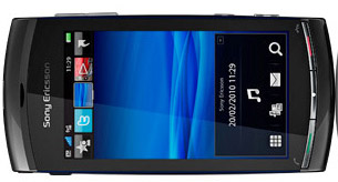
Reverse engineering the Sony Ericsson Vivaz high resolution 640 x 360 cellphone LCD
Welcome to another in my series of cellphone LCD reverse-engineering articles. In this article I’m going to present everything you need to hook up the high-resolution 640×360 LCD from the Sony Ericsson U5 Vivaz to your project.
About the phone and LCD
The Sony Ericsson U5 Vivaz LCD is a 3.2″ 640×360 TFT with a nice high pixel density of 229ppi. Replacement panels are available on ebay for as little as GBP 6.00.
Key to any reverse engineering effort is the ability to find the schematic for the phone in question. A bit of googling turned up the relevant repair manual and I was pleasantly surprised to see that the LCD connector had the 8080 interface signals that indicate the presence of an onboard controller.
Why the surprise? Well, every high-resolution display that I’ve investigated to-date has had either a parallel or MIPI-DSI interface designed to be connected to a system-on-a-chip (Soc) controller that would supply both pixel data and display timing signals. These interfaces are unsuitable for the small STM32 and AVR microcontrollers that we all enjoy programming because of the requirement to provide a frame buffer and display signals that are difficult to synthesize. The presence of an 8080 controller on this LCD definitely caught my eye. Time to order a panel.
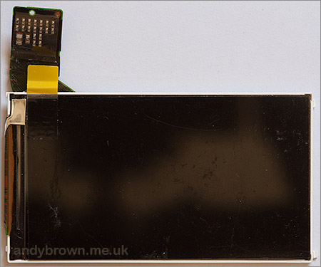
That’s the front view, let’s take a look at the back.
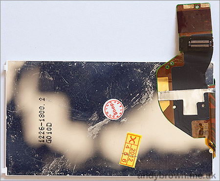
There’s nothing unusual about the panel compared to the others that I’ve reverse engineered in the past. The FPC is in a reasonable position and is a useful length.
The connector is a board-to-board type and there’s an array of SMD capacitors situated close to it.
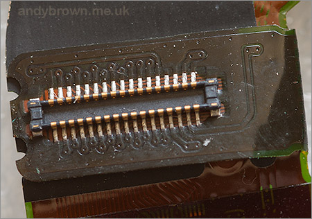
The connector
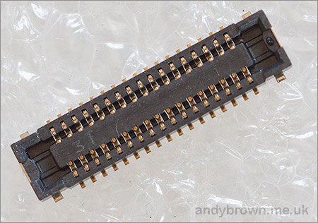
The second critical part of the reverse engineering effort is the ability to identify and source the FPC connector required by the panel. In this case the repair manual provided the necessary information. Right underneath the diagram for the LCD connector is a label AXE534124.

Click for a larger image
Off to Google I go and the answer is immediately located. It’s a 34-pin 0.4mm Panasonic AXE534124 and better still it’s in stock at digikey.com. I won’t try to link directly to it here as external links to shop pages tend to be brittle. Just go over to digikey.com and search for AXE534124.
Note that for reasons I don’t understand Digikey will not sell this connector off any site except digikey.com so if you’re not in the USA you must switch to use the USA site to make your order.
Soldering this connector was a little bit more fiddly than the others I’ve dealt with because the legs do not protrude very far from the connector body making it very likely that you’ll slip with your soldering iron at least once and melt a little bit of the body plastic.
The connector footprint
I designed a footprint for the connector using my copy of Protel, here’s how it looks.
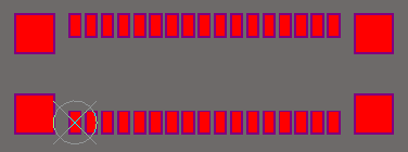
Now I know that a significant number of you will be using CADSoft Eagle as your design package so here are the dimensions from the footprint that you’ll need to create your own in Eagle. All the following positions and dimensions are in millimetres.
The pin size is 0.23 x 0.5 with a solder mask expansion value of 0.051. The pin with a crosshair on it is at (0,0). The pin immediately to the right is at (0.4,0). The pin directly above is at (0,2.4).
The pad size for the four supporting posts is 0.9 x 0.9 with a solder mask expansion of 0.051. Starting at the top-left and moving clockwise the positions are (-1,2.2), (7.4,2.2), (7.4,0.2), (-1,0.2).
The final part in the connector identification process is to try to figure out which way around it goes. I know from the schematic that the pins are arranged in two columns, A and B. Often I can use the position of the ground pins and check continuity between them with a multimeter to verify which pin is which. In this case that approach is thwarted because the the ground pins are arranged symmetrically across the connector.
I solved the problem by doing a little bit of cross-referencing. The schematic includes a block diagram of the main phone PCB:
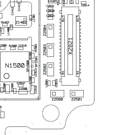
The LCD connector is labelled X2821 in the diagram and rather helpfully it has the position of the pins labelled on it. Now I needed to know which way the plug on the FPC connects into that connector so I searched around and found a video on youtube that showed how to disassemble the phone. The sequence where the presenter disconnected the LCD revealed all that I needed to know.
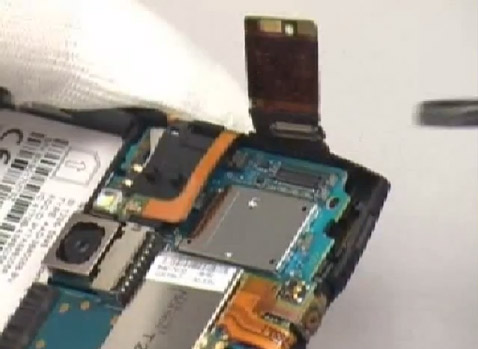
The frame grab shows the plug on the FPC in the correct orientation relative to the connector. Now I have all the information that I need.
Powering the backlight
The schematic shows that there’s a single pair of power lines connected to the backlight, LCD_BL_K and LCD_BL_A. That means that the LEDs that form the backlight are arranged in series and I’m going to need a step-up driver to power them. Every parallel LED configuration that I’ve seen has all the cathodes exposed for individual feedback into the constant current driver IC.
The schematic doesn’t tell me how many LEDs make up the backlight so I’m going to have to make an educated guess that it’s at least four but is more likely to be six. The NCP5007 device that I used to drive the backlight in the Nokia displays will not be sufficient because it’s limited to five LEDs so I need to choose something else.
The device I selected is the AP5724 from Diodes Inc. It’s available from Digikey in the SOT26 package that I selected for this design.
An early guess at the controller
Before designing a breakout board I decided to have a look around for datasheets that might belong to the controller. There were not many candidates. An exact match was the R61523 by Renesas. Another possibility was the SSD1963 by Solomon Systech that has flexible support for a large range of resolutions.
I decided to follow up on the Renesas option and tried some cross-referencing using Google to try to find any commercial relationship announcements between Sony-Ericsson and Renesas at about the time of the phone’s launch date. There was just such a press-release, dated around 2007. The case for the R61523 was getting compelling and I decided to run with it as the main candidate.
Flicking through the R61523 datasheet to the electrical specifications I found the desired voltage levels. TFT panels like these generally require two supply voltages, one for the digital IO (IOVCC) and one for the panel power (VCI). If you’re lucky then both fall within the same range and coincide with your MCUs core voltage.
I wasn’t so lucky with this one. IOVCC has a desired range of 1.65-3.6V which is fine but VCI’s range is 2.6-3.0V. I will be able connect up my 3.3V STM32 directly to the IOs but I’ll need to add a 2.8V LDO regulator to the design to supply VCI within its desired range.
A breakout board schematic
Now I’ve got hold of the schematic and the connector I have enough information to create a schematic for a breakout board.
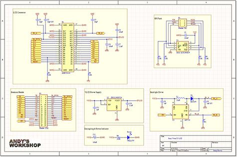
Click preview for a full size PDF
The schematic is divided into annotated sections, let’s take a look at each one in turn.
The VLCD power supply
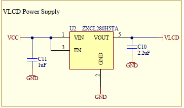
I mentioned earlier in this article that the R61523 was specified to require a 2.8V panel power supply and the datasheet indicates that the maximum current consumption will be a mere 4mA. Any LDO regulator will handle this load but an additional requirement imposed by my design is that the dropout voltage must be less than 0.5V because the input to the regulator will be 3.3V.
I chose the ZXCL280H5TA from Diodes Inc. in SC-70 format. The dropout voltage at 4mA is so small it’s hard to determine from the chart in the datasheet. It’s somewhere around 5mV.
Decoupling and power indicator
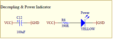
The board includes a 100µF capacitor for low frequency decoupling and a 1206 footprint amber LED for a power indicator. The series resistor is calculated to allow about 4mA through the LED which is plenty for an indicator.
Backlight driver
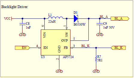
My (guessed) requirements for the backlight are discussed earlier in the article. My assumption is that there are six backlight LEDs which I know are connected in series and that means that I need an appropriate step-up driver.
The AP5724 from Diodes Inc. satisfies the requirements and my implementation is straight from the example application circuit in the datasheet. The feedback resistor, R7, has a value of 5.1Ω which results in a constant output of 20mA.
The LCD connector
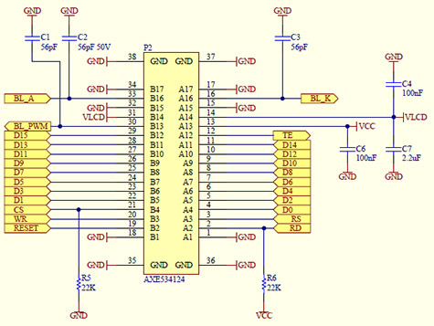
The circuitry around the LCD connector mirrors that which I found in the schematics for the actual phone. A familiar selection of capacitors provide decoupling on the supply lines. The BL_A and BL_K 56pF capacitors are rated at 50V because of the high voltage on those lines. RD and CS are pulled up and down, respectively, because they are rarely used in designs and so can be left disconnected if required.
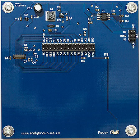
The breakout header
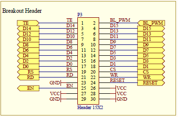
The breakout header is a 15×2 header with the standard 2.54mm pitch. Here’s a table that describes how to hook it up to an MCU.
| Pin | Function | Description |
|---|---|---|
| TE | Tearing effect | VSYNC and optionally also HSYNC output. Used for sychronising your drawing with the LCD refresh to avoid flicker. |
| BL_PWM | Backlight PWM | Optional output for a PWM signal that can be used to dim the backlight. Connect to the EN pin if this functionality is used. |
| D0..15 | Data bus | 16-bit data bus for commands and data. |
| RS | Register select | Set high when writing data or low when writing a command. The datasheet calls this line DCX. |
| CS | Chip select | The controller will ignore you unless this line is low. Pulled down by default. |
| WR | Write enable | Active low write strobe. |
| RD | Read enable | Active low read strobe. Reading is hugely slower than writing and so is not often used. Pulled up by default |
| RESET | Hard reset | Active low hard reset. |
| EN | Backlight enable | Tie to VCC to fix the backlight to maximum (an adjacent pin is provided to enable easy connection with a jumper). Alternatively supply a PWM signal from your MCU to dim the backlight. Better still, connect to BL_PWM and program the controller to provide the PWM signal. |
| VCC | 3.0 to 3.3V | Power for the LCD, inputs to the AP5724, flash and ZXCL280H5TA. |
| GND | Ground | Connect up one of the GND pins to your circuit’s ground. |
SPI flash
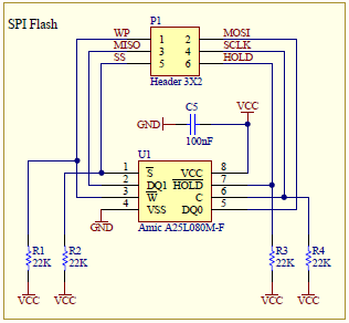
I have lots of space on the board so I decided to include a separate breakout area for a SPI flash IC that can be loaded up with graphics, fonts and other resources that might be required by a program. The SOIC-8 footprint is designed to take any 208mil ‘wide’ package but will happily also accept the smaller 150mil footprint. SPI flash ICs pretty much all have the same pinout so you can insert any one that fits your requirements.
Bill of materials
Here’s the complete bill of materials for the schematic.
| Code | Value | Footprint |
|---|---|---|
| C1,C2,C3 | 56pF 50V | 0603 ceramic |
| C4,C5,C6 | 100nF | 0603 ceramic |
| C7,C10 | 2.2µF | 0603 ceramic |
| C8,C11 | 1µF | 0603 ceramic |
| C9 | 1µF 50V | 0805 ceramic |
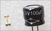
| C12 | 100µF | Electrolytic |
| R1,R2,R3,R4,R5,R6 | 22kΩ | 0805. Exact value not important. |
| R7 | 5.1Ω 1% | 0805 |
| R8 | 390Ω | 0805 |
| PWR LED | Yellow | 1206 |
| D1 | Schottky | SOD-123. Many types can be used. |
| L1 | 22µH | Many types can be used. |
| P1 | 3×2 male | 2.54mm |
| P2 | AXE534124 | 0.4mm x 34 |
| P3 | 15×2 male | 2.54mm |
| U1 | any SPI flash | SOIC-8 (208 or 150mil) |
| U2 | ZXCL280H5TA | SC-70 |
| U3 | AP5724 | SOT26 |
Building the PCB
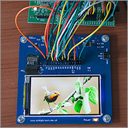
Many of my previous designs have featured a wrap-around design whereby the LCD occupies one side of the PCB and the flex cable wraps around to the connector on the other side that also houses the circuitry. I could probably have done that this time as well but decided instead to opt for a larger 10x10cm PCB and fit the whole design on to one side including space for M3 screw mount holes.
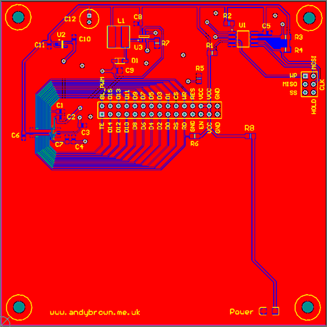
The front side has all the components and a vacant space down at the bottom that’s calculated to hold the LCD panel mounted on some double-sided sticky pads.
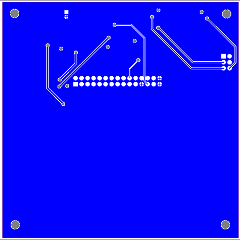
Click either image for a PDF
Given the spacious size of PCB the routing did not present any challenges. Now with the design complete it’s time to send it off to one of the Chinese online sellers for manufacturing. In the past I’ve used ITead Studio and occasionally Seeed Studio. This time I used a relative newcomer, Elecrow, because they don’t charge extra for coloured PCBs and I wanted mine to be blue.
I uploaded my design and waited the three or so weeks that it takes to arrive. I had cause to visit Shenzhen, China on business during the waiting time and could have dropped in and picked it up while I was there!
Anyway, the PCBs arrived in the post and as usual they were perfectly made.
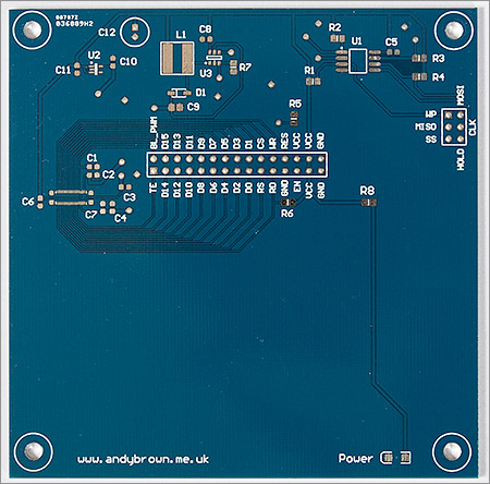
My process for building the PCB involves several stages. First I flux and tin the pads so they all have little solder bumps on them. The flux used for this stage is the highly active Fluxite brand. The board is then washed to remove all trace of the corrosive flux before doing anything else.
I then reflow the ICs and fine-pitch connector using a hot plate and then reflow the discrete components using a hot air gun. Then I inspect my work under a microscope and use a regular fine-tip iron to touch up any joints that have not reflowed correctly. Finally the through-hole components are soldered using a regular iron and then the board is washed in soapy water, rinsed and left to dry for 24 hours.
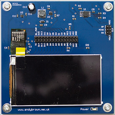
Here’s a photograph of the completed board before the LCD is attached.
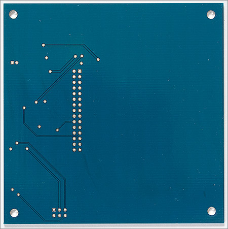
And here’s the board again with an LCD attached this time. The protective peel-off plastic film is still attached to the front of the LCD.
Programming the controller
Now that I’ve got a breakout board the first thing to do is to verify my guess that the controller is a Renesas R61523. The datasheet defines a command Device Code Read that will return four bytes that identify the controller.
If you’re looking to write your own R61523 driver then do note that many of the useful commands are locked after reset and require you to send the MCAP command with a paramter of 4 to unlock them.
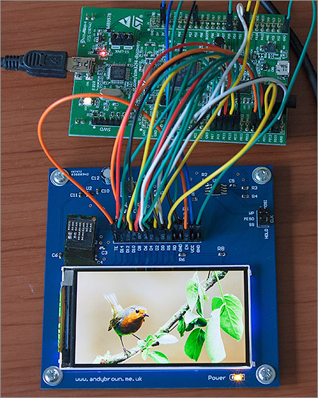
I hooked up the screen to my STM32 F103 development board and wrote some code to reset the board and issue the Device Code Read command. Great news, it worked and it returned the expected sequence of bytes. Now I know for sure that I’m dealing with an R61523 I can go ahead and write STM32 and Arduino drivers.
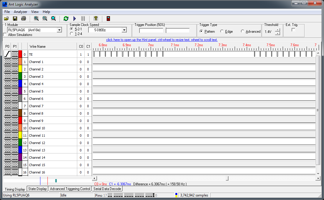
The TE output signal
LCD controller manufacturers use the acronym TE or Tearing Effect for signals that the rest of the world calls VSYNC and HSYNC. LCD panels require a signal to tell them where the top of the display is (VSYNC) and another one to tell them where the start of each line is (HSYNC).
If you need to a produce a display that doesn’t flicker (or ‘tear) then you have to do your drawing when the LCD is not busy taking data from the video RAM and sending it to the screen. You can do this by starting your drawing when you receive the VSYNC signal and using that vertical blanking time to write out your data. It’s not as powerful as double-buffering but on a display like this it’s all you’re going to get.

Click for larger
The above image shows the TE signal configured to output a pulse on VSYNC only. We can see that the LCD is running with about a 60Hz refresh rate.
Click for larger
The above image shows the TE signal configured to output a pulse on VSYNC and HSYNC. Clearly there are a lot more pulses in this mode.
An stm32plus driver
I tackled the STM32 driver first and it wasn’t long before I had it up and running. 16, 18 and 24 bit colour depths are all supported in portrait or landscape mode. Tearing effect output (vsync and/or hsync) is supported as is the controller-generated PWM output for backlight dimming. On the STM32 this saves us programming a timer peripheral to provide the backlight dimmer.
I was pleasantly surprised with the quality of the clone screen that I got on ebay. It is bright and contrasty with a wide viewing angle and high-fidelity colours. There is a visible increase in the quality of gradients when moving up from 16 to 18 and 24 bit colours meaning that even the clone screen isn’t faking the higher colour depths.
For comparison purposes I also bought a display advertised as ‘original’ for a few pounds more. The original improves slightly on the clone in the definition of the blacks. Blacks remain a deep black even with the backlight on the full 20mA current whereas the clone tends to go a deep grey instead. Given the small difference in price I would recommend going for an original display panel because even though I had good luck with the clone display that does not mean that all clones will be good.
stm32plus 3.0.2 includes a driver for all the R61523 modes and a graphics library demo that will work on the F103 or F4. Naturally the F4 is the top performer with outstanding blink-of-an-eye fill rates but the F1 is not far behind at all.
A note on the STM32F4 Discovery
This is a high speed LCD. The F4 is a high speed MCU. Together they make a perfect couple but like many perfect couples their relationship can be a fragile one. If you intend to wire this LCD board up to the F4 Discovery board then you must take care with the quality of your wiring. Remember that you are creating a high-speed bus, and this advice applies equally well to all high-speed MCUs.
- Keep your wires short and all of equal length.
- Avoid a ‘rats nest’. Try to avoid twisted and crossed over wires.
- Ensure your wires mate well with the pin headers. For god only knows what reason ST decided to put short pins on the ‘business side’ of the discovery board making wired interconnects precarious.
If you get a ‘glitchy’ display with random small areas of corruption then it’s most probably your wiring. I’ve been known to wire and rewire the discovery board three times to get a 100% reliable connection. Maybe my interconnects are junk, I did get them on ebay after all 🙂
You can see the graphics library demo running glitch-free on the STM32 F4 Discovery board in the following video. The display is running in 24-bit mode (two 16-bit transfers per-pixel).
An Arduino Mega driver
A few months ago I presented a generic 16-bit LCD adaptor that can be used to connect panels such as this to the Arduino. I connected up the R61523 to this adaptor and began writing a driver that would use the highly optimised GPIO access mode that I presented in the adaptor article. With 640×360 pixels to drive every clock cycle counts and a poorly optimised driver will result in a sluggish user experience.
Version 3.0.2 of my xmemtft library has support for the 64K colour mode in portrait and landscape mode. You can see for yourself how well the library performs in the following video.
Gamma setting
After a reset both the clone and the original panels are slightly too dark and benefit from a custom gamma curve to lift the bottom end of the grey scale up a bit so that detail in the shadow areas of photographs is not lost.
The R61523 is extremely flexible with its gamma settings and you can program separate levels for each of the RGB components if you need to. I didn’t need to adjust the colours so I flattened the 78 different parameters into just 13 levels designed to view the curve as greyscale.
In the demo code the curve is declared and applied like this:
uint8_t levels[13]={ 0xe,0,1,1,0,0,0,0,0,0,3,4,0 };
R61523Gamma gamma(levels);
_gl->applyGamma(gamma);
In the driver code I apply the curve like this:
/**
 * Apply the panel gamma settings
 * @param gamma The collection of gamma values
 */

template<Orientation TOrientation,ColourDepth TColourDepth,class TAccessMode>
inline void R61523<TOrientation,TColourDepth,TAccessMode>::applyGamma(const R61523Gamma& gamma) const {

  applyGamma(r61523::GAMMA_SET_A,gamma);
  applyGamma(r61523::GAMMA_SET_B,gamma);
  applyGamma(r61523::GAMMA_SET_C,gamma);
}


template<Orientation TOrientation,ColourDepth TColourDepth,class TAccessMode>
inline void R61523<TOrientation,TColourDepth,TAccessMode>::applyGamma(uint16_t command,const R61523Gamma& gamma) const {

  uint8_t i;

  _accessMode.writeCommand(command);

  // positive and negative

  for(i=0;i<2;i++) {
    _accessMode.writeData(gamma[0]);
    _accessMode.writeData(gamma[1]);
    _accessMode.writeData(gamma[3] << 4 | gamma[2]);
    _accessMode.writeData(gamma[5] << 4 | gamma[4]);
    _accessMode.writeData(gamma[6]);
    _accessMode.writeData(gamma[8] << 4 | gamma[7]);
    _accessMode.writeData(gamma[10] << 4 | gamma[9]);
    _accessMode.writeData(gamma[11]);
    _accessMode.writeData(gamma[12]);
  }
}
The onboard backlight PWM driver
In nearly all my previous LCD driver projects I have used the MCU to generate a PWM signal that is connected to the LCD driver’s EN pin in order to dim the backlight. The R61523 includes an onboard PWM generator that does the job for us and saves us an output pin and a timer peripheral on the MCU. The controller will even do a smooth transition between backlight levels.
Both the stm32plus and the Arduino drivers come with a backlight driver class that allows you to customise the PWM frequency, polarity and whether you want the smooth transition mode to be enabled or not.
Using the onboard SPI flash
The development board that I created for the LG KF700 was the first to include a SPI flash IC that could be used to store resources such as graphics and fonts.
This time around I have included the Spansion S25FL208K 8Mbit flash IC on board. The S25FL208K is a standard SPI flash device so it can be programmed using the spi_flash_program example code included with stm32plus.
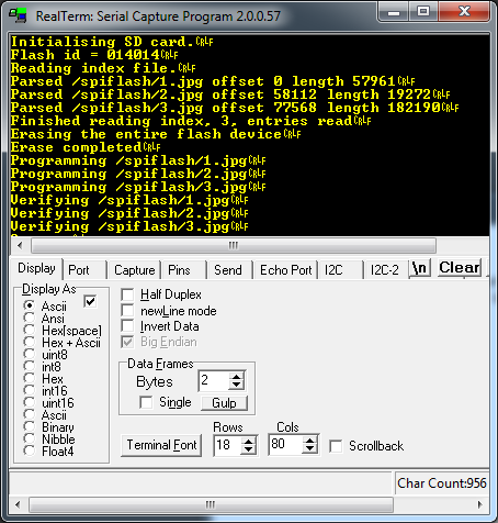
The example code reads files from an SD card, writes them to the flash IC at the locations you specify and prints out status messages to a USART port.
Print your own PCBs
Want to have a go at assembling one of these boards yourself? Head on over to my downloads page and grab yourself a copy of the zip file containing the Gerber CAM files. An online service such as that offered by Seeed Studio, ITead Studio or Elecrow can be used to get 10 copies for a very reasonable price.
Update: another panel type found
I recently bought another clone panel on ebay to mount on a second board that I made up. When this panel arrived the first thing that I noticed was that the breakout area on the FPC cable where all the capacitors are mounted looked quite different to the original Sony panel.
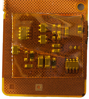
If you compare this to the first image in this article you can see that the grid of capacitors is replaced by a selection of capacitors and ICs. Interesting. I hooked it up to the board and fired up some test code.
As well as flickering wildly the displayed image was compressed on to one side of the screen and appeared to be mirrored on the other side. I thought the screen was broken but decided to investigate further to see if it was something I could fix in code. It was.
To understand how the fix works it helps to understand how the R61523 is designed. The R61523 has a region of registers that it calls manufacturer commands. These registers define parameters specific to the physical panel such as power settings and panel driving parameters.
A region of non-volatile RAM (NVRAM) is programmed at the factory with the correct values for the manufacturer commands and the R61523 reads the NVRAM and applies the values after the device is reset. This allows the R61523 to be used in panels sourced from many different manufacturers.
I wrote some code to read out the manufacturer command values from the original Sony panel and compared them to the values obtained from this latest clone. The original panel had some values that were different from the power-on defaults documented in the datasheet indicating that its NVRAM had been programmed at the factory. The clone only had the standard R61523 power-on defaults indicating that it had not been programmed.
I sat down and went through the registers that could possibly cause the mirrored display and flickering that I observed and soon found the two settings. They were panel_driving_setting (C0h) and power_setting_common (D0h).
The thing I don’t understand is how these panels could ever work in the actual phone because the phone will only be coded to work with the originals which load up the parameters correctly from NVRAM. Maybe they don’t work in the phone? It wouldn’t be the first time that ebay sellers have been sold a pup by their Chinese suppliers.
The correct additional initialisation code for these panels is shown below:
// this panel needs SM=1 (first parameter). the others are the same
// as the original Sony. if SM is not set to 1 the image will appear
// duplicated on the left and right of the display.

TAccessMode::writeCommand(r61523::PANEL_DRIVING_SETTING);
TAccessMode::writeData(0x8);
TAccessMode::writeData(0x9f);
TAccessMode::writeData(0);
TAccessMode::writeData(0);
TAccessMode::writeData(2);
TAccessMode::writeData(0);
TAccessMode::writeData(1);

// this panel needs VC2/VC3 set to 0x5 (second parameter). This is the
// optimum setting that reduces flicker. the other values are the same
// as the original Sony.

TAccessMode::writeCommand(r61523::POWER_SETTING_COMMON);
TAccessMode::writeData(0);
TAccessMode::writeData(0x55);
TAccessMode::writeData(0xc0);
TAccessMode::writeData(0x8f);
I have modified my stm32plus and Arduino drivers to cope with this panel. Following the convention that I established with my Nokia drivers this panel can be used by appending _TypeB to the driver name. For example, R61523_Landscape_16M_TypeB on the STM32 and R61523_Landscape_64K_TypeB on the Arduino. I have pushed these changes to their respective github repo on the master branch.
Resources
This entire project is open source. I hope I’ve given you enough information and indeed inspiration within the narrative to get on and build your own halogen reflow oven. Please visit my downloads page to get copies of the Gerbers that you can use to print your own boards. The source code to the firmware is available on Github.