


Reverse engineering the LG KF700 480 x 240 widescreen cellphone LCD
Hello and welcome to my first published non-Nokia cellphone LCD reverse-engineering effort. All my articles in this series focus on bringing you all of the details that you would need in order to connect a low-cost cellphone LCD to an MCU for use in your own projects. This one is no different. I will explain the pinout and the signals. I will tell you about the connector and where you can buy it and I will tell you about the controller IC and of course I will give away the complete source code driver for that controller.
Let’s get started.
The LG KF700
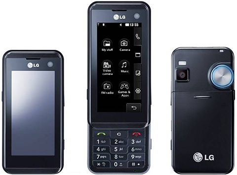
The KF700 was released in 2008 and is now a discontinued model. It featured a 3.0 inch 480×240 LCD in an unusual wide-screen format with an aspect ratio of 2:1. I noticed that replacement LCDs were available cheaply for it on ebay and so I set about trying to find the schematics.
That part was easy, a simple google search for ‘KF700 schematic’ will yield the set of repair manuals including the all-important electrical information.
The schematic document is very informative and part of me is very thankful to LG for making this easier than it could have been but another part relishes the challenge and this one was less of a challenge than the others have been.
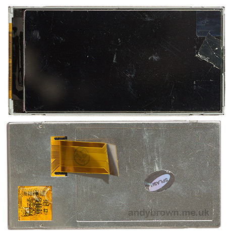
The composite photograph shows how a replacement screen looks when it arrives from ebay. There’s a protective film over the front and the back exposes the FPC cable and connector.
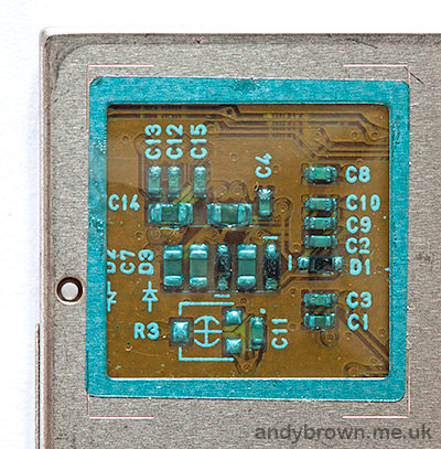
A small exposed square houses some unknown circuitry that, on the genuine LG part includes a green LED that lights up when power is applied.
Identifying the interface mode
If this LCD is going to stand any chance at all of being usable by a small microcontroller then it’s going to need to have an embedded controller IC. If it has a parallel or an MDDI interface then we are out of luck because those modes need an external framebuffer and a powerful microcontroller.
As luck would have it, LG published the following block diagram on page 58 of the service manual.
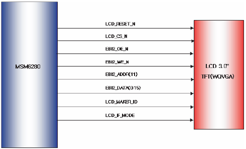
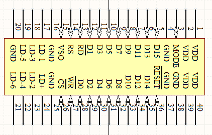
Those signals identify that there’s a controller IC present. Good. Next thing we need to do is identify the connector and its pinout. Again, LG are to be thanked for publishing the connector schematic on the very next page.
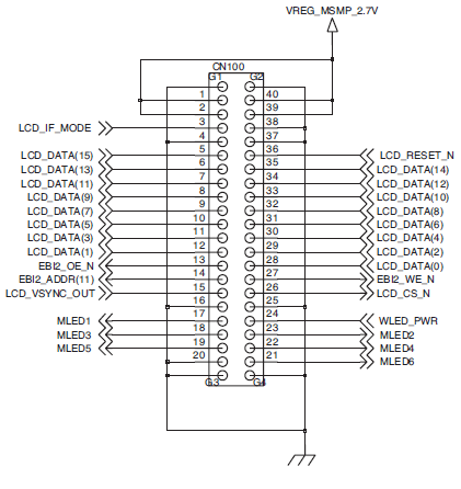
It’s a 40-pin board-to-board connector and all the expected signals are there plus a few that I’m going to have to take an educated guess about. I’m going to assume that EBI2_ADDR(11) is the register select (RS or D/CX) signal. At this stage I’ve no idea what LCD_IF_MODE is going to do but it only has two states so it won’t be much effort to try both.
One strong positive is that the presence of six backlight LED outputs tells us that the backlight is wired up in a parallel configuration, negating the need for a step-up DC/DC converter. A simple resistor could be used to regulate the current.
Where to buy the connector
Often this is a tricky one, even if one can identify the connector it can be impossible to find a supplier willing to sell it in small quantities. LG to the rescue again. In the appendix to the service manual they tell you the part number.
It is ENBY0045701 and it’s available from your local LG spare parts supplier. I used http://www.4ourhouse.co.uk/. Let’s take a close look at it.
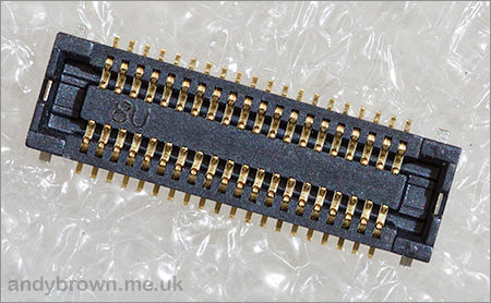
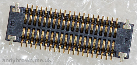
It’s a 40-pin receptacle with a 0.4mm pin pitch making it difficult to hand-solder but no problem for reflow on a hot plate.
The connector orientation
With a spare LCD to hand it’s not too difficult to determine the correct connector orientation, i.e. locating pin number 1. The way I do that is to find the ground connections on the schematic and then examine the connector under a microscope.
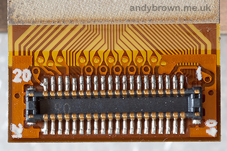
Typically the ground connections will connect directly into the ground plane embedded in the FPC tail making them simple to identify. Once I think I’ve found them I’ll use the continuity checker on my multimeter to verify that all the pins that I think are ground are connected together.
I’ve mentioned before that one should not trust the pin numbers that are silkscreen’d on to the connector because they often do not match the schematic, and that’s the case this time. The pin labelled #1 on the connector photograph above is actually pin #40 on the schematic.
A connector footprint
I used an old copy of Protel to do the design for this project and I realise that many of you will be using CADSoft Eagle so I’m going to give you a little help with the connector footprint.
First, here’s the schematic and footprint view.
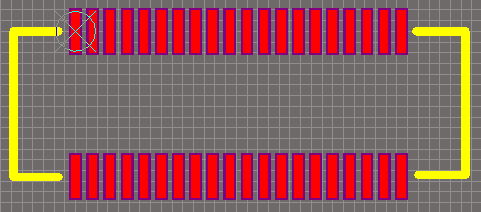
Each pad is 0.2mm x 1mm and I have specified a solder-mask expansion value of 0.051mm.
The pad at the top-left with the crosshair on it is centered at position (0,0). The pad to the right of it is at position (0.4mm,0).
The pad at the bottom left is at position (0,-3.38mm). The pad to the right of it is at position (0.4,-3.38mm).
I have not included pads for the four supporting tabs. If you do include them then connect them to your GND net.
The three yellow lines that make up the silkscreen on the left are 0.2mm thick and have the following (x,y) -> (x1,y1) values in mm:
(-1.45,0) => (-0.4,0)

(-1.45,-3.4) => (-1.45,0)

(-1.45,-3.4) => (-0.4,-3.4)
The three yellow lines that make up the silkscreen on the right are 0.2mm thick and have the following (x,y) -> (x1,y1) values in mm:
(8,0) => (9.1,0)

(9.1,-3.4 => (9.1,0)

(8,-3.35) => (9.1,-3.4)
Hopefully that’s all you need to create a compatible footprint in Eagle or any other package.
Identifying the controller
Traditionally this has always been the hardest part of any reverse engineering effort involving probing registers and trying to work out how they match up with known controllers. Thankfully though, LG have again been generous in the service manual. On page 58 it says this:
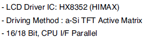
There it is, handed to us on a plate. The datasheet for the HX8352A is readily available on the internet and a quick scan through it tells me that it’s somewhat similar to the HX8347A that I already know quite well.
With the controller identified, it’s time to design a development board.
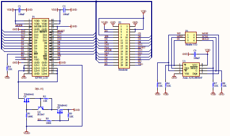
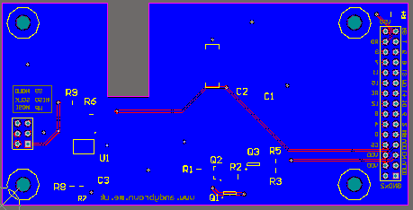
A development board schematic
Click thumbnail for PDF
The schematic contains the basics for the breakout of the connector and a few extras that I decided to include for fun. Let’s go through them in detail.
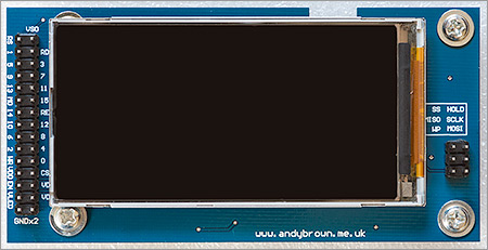
The 30-pin breakout header
The 2.54mm, 30-pin breakout header has the following pinout.
| Pin | Function |
|---|---|
| RS | LCD register select. |
| RD | LCD read control. Pulled up to VDD. |
| WR | LCD write control. |
| CS | LCD chip select. Can be grounded. |
| 0..15 | LCD 16-bit data bus. |
| VSO | Vertical Sync output. |
| MO | Colour mode selection. GND=64K, VDD=262K |
| RE | LCD reset. |
| EN | LCD backlight enable. Tie to VDD for full brightness or apply PWM signal to control it. |
| VDD | 3.3V power input. 3.3V is the limit, do not exceed it. |
| GND | Ground. |
| VLED | Voltage source for constant current backlight generator. Normally tie to VDD unless using STM32 F4 Discovery board in which case should be connected to a 5V output from that board. |
The LCD power supply
LCD controllers normally take two power supply inputs, one for the panel and one for the digital signals. In this case they appear to be bonded together on pins 40 and 39 and the phone supplies them with 2.7V.
A quick glance at the HX8352A datasheet reveals that the recommended ranges for the power supplies are Vcc = 2.4 ~ 3.3V and IOVcc = 1.65 ~ 3.3V. My target microcontroller is going to be the STM32 running at 3.3V so I will not be needing any level conversion as 3.3V is at the top end of both the recommended ranges.
The backlight power supply
The backlight is comprised of six white LEDs in parallel so we do not need a step-up converter and could in theory drive it with a single current-limiting resistor. The LEDs probably have a forward voltage of around 3.2V each and there are calculators out there on the web that will do Ohm’s law and tell you the value of the resistor that you should use.
However, for tasks like this I much prefer a constant current source over a simple resistor. There are integrated devices on the market that exactly match what I need, for example the CAT3649 by OnSemi. I evaluated that device and even bought a few to play with. In the end though, I decided to go with the circuit in this instructable.
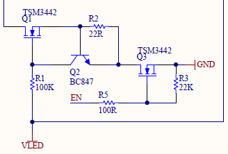
The circuit has the advantage of requiring only a handful of very low-cost parts, two MOSFETs, a transistor and four resistors. The current-setting resistor is calculated for a current of 20mA. VLED is the input power supply, 3.3V in all my tests. If you plan to use this circuit on the STM32 F4 Discovery board then VLED should be connected to 5V. The 3V outputs from the board are not high enough to drive the backlight circuit and if you try then the display will be quite dimly lit.
My circuit differs slightly from the instructable in that I’ve added a second MOSFET, Q3, so that we can control the brightness of the backlight with a PWM signal from a microcontroller through the ‘EN’ signal. The gate of Q3 is pulled down to ensure it stays off until needed and the MCU pin is protected from unwanted current discharge from Q3’s gate capacitance by a 100Ω resistor, R5.
The RD line
RD is only used if you want to read data from the framebuffer. Read cycles are very much slower than write cycles and so this line is hardly used. Therefore it’s pulled up to VDD in my design.
The SPI flash
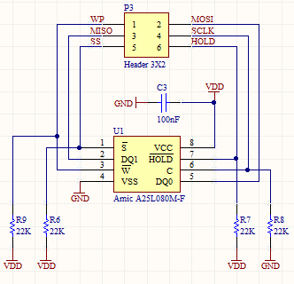
Since this is going to be quite a large breakout board I decided to include the necessary footprints for a SPI flash IC circuit that can be used to store such things as graphics and fonts that can then be utilised by the software driver.
The SOIC-8 SPI flash footprint pinout is a de-facto standard across manufacturers. I’ve included the Winbond W25Q16DW as an example but any device in the 209 mil SOIC-8 format is likely to be compatible.
Bill of materials
Here’s the complete BOM for this project:
| Label | Value | Footprint | Comment |
|---|---|---|---|
| C1,C2,C3 | 100nF | 0603 | Decoupling |
| P1 | ENBY0045701 | 40×0.4mm | FPC connector |
| P2 | 2×15 | 2.54mm | LCD breakout |
| P3 | 2×3 | 2.54mm | Flash breakout |
| Q1,Q3 | TSM3442 | SOT26A-6 | Logic MOSFET (use any) |
| Q2 | BC847 | SOT23-3 | Small signal transistor |
| R1 | 100kΩ | 0805 | |
| R2 | 22Ω 1% | 0805 | Current setting |
| R3,R4,R6,R7,R8,R9 | 22kΩ | 0805 | Pull up/down (value not important) |
| R5 | 100Ω | 0805 | MCU protection |
| U1 | SPI flash | SOIC-8 209mil | Use any compatible IC |
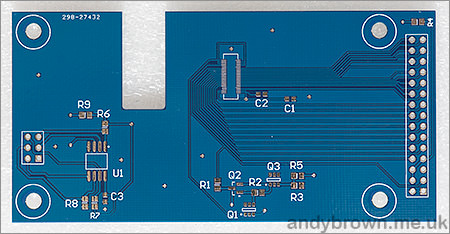
The PCB CAD
The target maximum size for this design is 10x5cm so I’ve got quite a lot of leeway to layout the components and include M3 screw holes to use as mounting feet. Here’s the front.
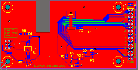
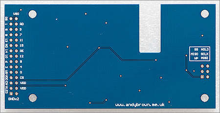
The only constraint is the slot required to accomodate the FPC tail so it can thread through the board and plug into the socket located on the component side of the board. Here’s the back layer.
Getting the slot and connector in the correct location is the most tricky part. I measured where I thought the location would be and then tested it by printing out a 1:1 paper copy of the layout, cutting out the slot and offering up the LCD to ensure that it would fit.
The manufactured board
Regular readers will know that I usually use ITead Studio as the manufacturing service. Other service providers exist such as Seeed Studio and one I hadn’t heard of before, Elecrow.
I decided to give Elecrow a try since they were offering colour PCB printing at no extra cost. I was pleased with the result and suspect that they’re using the exact same fabrication plant as Seeed and ITead.
Building the board
My technique for building a board like this involves several stages of preparation, reflow and hand-soldering. Firstly I use a highly active flux (Fluxite) to tin the pads because I find that this flux is ideal for drag-soldering with a normal iron across the tiny 0.4mm pitch pads without creating any bridges or solder spikes. When this is done the board is thoroughly cleaned to remove all trace of the flux – it’s corrosive and should not be left on the boards. After cleaning only water-soluble flux designed for electronics is used.
With the board prepared I use a paste flux to lightly grease the IC pads and then place the connector and the ICs into position using a microscope to ensure accuracy. I then use a hot plate to reflow the board until I see the components ‘sit down’ into the little solder bumps. The next stage is to touch-up the reflowed joints with a normal iron under the microscope – there’s always one or two legs that didn’t quite drop into the solder while it was on the hot plate.
Finally the discrete 0603 and 0805 components are reflowed into place using a hot-air gun and any through-hole devices (e.g. pin headers) get soldered on with a regular iron.
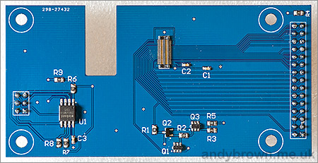
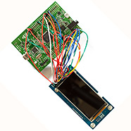
Here’s the component-side of the board after assembly. The screen is designed to fit on the other side with the FPC cable wrapping through the large slot and mating with the connector. Although the 40-pin 0.4mm connector looks a nightmare to fit I did not find it any more difficult than the 24-pin Nokia connector that I’ve worked with in the past. I wouldn’t like to try it with just an iron though; reflow makes it so much easier.
Here’s the finished article with the LCD fitted and (thankfully) mating correctly with the socket on the component side. Double-sided sticky pads serve to both fix the LCD in place and lift it up above the heads of the screws that are used to raise the components on the underside of the board off the table.
Now the hardware looks great, on to the software.
Programming the LCD controller
As mentioned earlier in this article, LG were kind enough to fess up to the controller being an HX8352A in the service manual. The pinout looks familiar enough with just a few pins in there that are not part of the of 8080 bus.
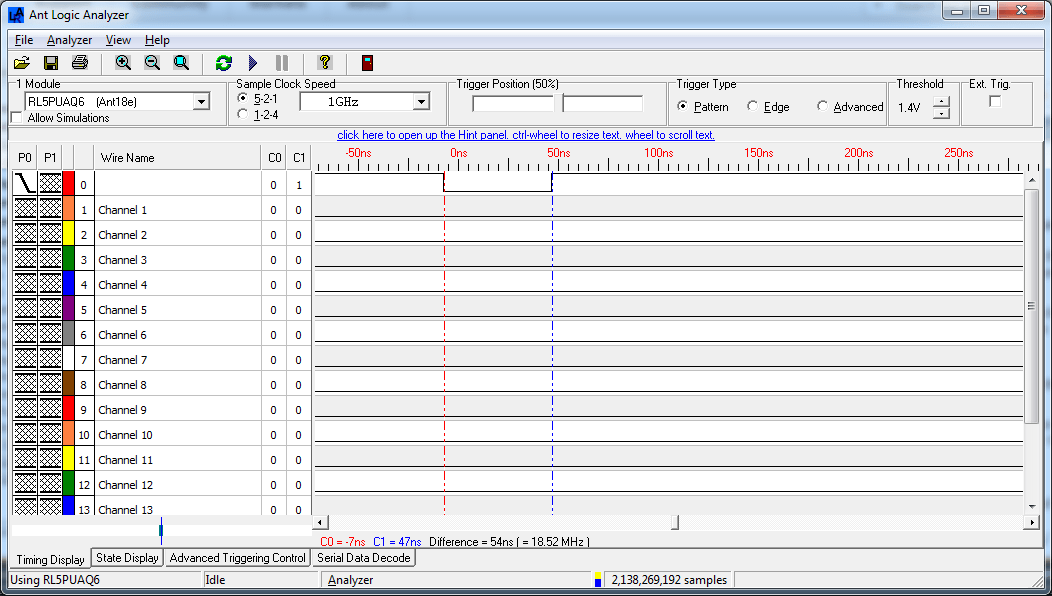
Firstly there’s the LCD_VSYNC_OUT pin. This one looks like it’s going to be the pulse that’s emitted at the start of the frame’s vertical blanking period to enable the microcontroller to synchronise its drawing to avoid the ‘tearing effect’, which co-incidentally is the name that this pin is often given by other controllers. Let’s jump forward a bit and see the signal that we get from this pin with a logic analyser.

Here we can see the vsync pulse being emitted with a frequency of 62.72Hz which corresponds to the refresh rate of the display.
The other unusual pin is the LCD_IF_MODE pin. It took me a while to catch on to this one. If you drive it low then the controller runs in 64K colour mode. If you drive it high then it runs in 262K mode. Every other controller that I’ve seen does this with a register setting and it was only when I noticed the lack of such a setting in the HX8352A datasheet that I twigged what this pin was for.
Writing the driver was fairly straightforward, aided and abetted by Himax’s application note that can be found online. In it they give some sample initialisation sequences which I adapted to this screen’s characteristics by changing the oscillator frequency to an appropriate value.
An stm32plus driver
I built a number of drivers for the STM32 F1 and F4. The first one uses the FSMC to drive the LCD bus in the same way that I’ve always done in the past. This performs well, especially on the F4, and is really easy to program. You can see the example code here on github. The FSMC access mode supports 16 and 18 bit colours using the following driver names:
LG_KF700_Landscape_64K
LG_KF700_Landscape_262K
LG_KF700_Portrait_64K
LG_KF700_Portrait_262K
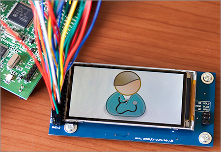
Here’s a photograph of the LCD connected to the STM32F4 Discovery board via the FSMC peripheral and running my graphics library demo.
The optimised stm32plus GPIO access mode
If you’re a regular reader of these articles then you’ll remember how I developed an optimised Arduino GPIO driver for 16-bit LCDs that achieved a very high fill-rate thanks to some assembly language trickery. Well, I’ve ported that technique to stm32plus for the F1 series of MCUs in the form of a Gpio16BitAccessMode template.
This GPIO driver means that not only can the F1 almost keep up with the F4 speed-wise, but it can also be used on devices that do not have the FSMC peripheral.
/**
 * Forward declaration for the template specialisations. These drivers
 * are highly optimised assembly language implementations designed to
 * extract the maximum performance from a GPIO based design. Each one
 * has been hand-tested and timed with a logic analyser to ensure it
 * meets its timing requirements.
 */

template<class TPinPackage,
         ColourDepth TColourDepth,
         uint16_t TClockFrequency,
         uint16_t TLow,
         uint16_t THigh>
class Gpio16BitAccessMode;
The basic idea is the same as the Arduino. Of course the assembly language is different and I have to provide specialisations of the access mode to suit the core clock and the write-cycle timing requirements of the LCD controller because, unlike the Arduino, the STM32 can drive the write-cycle faster than the controller can handle so I have to slow it down by a degree suited to the core clock speed of the target MCU. Gpio16BitAccessMode only uses raw GPIO and so it will work on devices that do not have the FSMC peripheral.
The additional complexity of having an instruction pipeline makes timing computation difficult as the same instruction can perform differently depending on its context. Having a logic analyser is critical to getting this right. For example, the method used to perform a 100ns write-cycle for one 16-bit data value on a 72Mhz MCU is shown here. The write cycle is divided 50ns low and 50ns high.
template<class TPinPackage,ColourDepth TColourDepth>
inline void Gpio16BitAccessMode<TPinPackage,TColourDepth,72,50,50>::writeData(uint16_t value) const {

  __asm volatile(
    " str  %[value], [%[data]]          \n\t"         // port <= value
    " str  %[rs],    [%[cset], #0]      \n\t"         // [rs] = 1
    " str  %[wr],    [%[creset], #0]    \n\t"         // [wr] = 0
    " mov  r0,       r0                 \n\t"         // burn 2 cycles so we meet the timing requirements
    " mov  r0,       r0                 \n\t"
    " str  %[wr],    [%[cset], #0]      \n\t"         // [wr] = 1
    :: [creset]    "r" (_controlResetAddress),        // the control reset address
        [cset]     "r" (_controlSetAddress),          // the control set address
        [data]     "r" (_portOutputRegister),         // the data port
        [wr]       "r" (TPinPackage::Pin_WR),         // WR pin bit
        [rs]       "r" (TPinPackage::Pin_RS),         // RS pin bit
        [value]    "r" (value)                        // input value
  );
}
Hooking up a logic analyser shows the signal is performing as expected:
As with the Arduino driver, the main performance boost is found in the unrolled writeMultiData() function. writeMultiData() takes advantage of the data value already being present on the bus lines and just toggles the WR line as fast as we are allowed in order to transfer blocks of data.
template<class TPinPackage>
inline void Gpio16BitAccessMode<TPinPackage,COLOURS_16BIT,72,50,50>::writeMultiData(uint32_t howMuch,uint16_t value) const {
  __asm volatile(
      "    str  %[value],   [%[data]]                 \n\t"     // port <= value
      "    str  %[rs],      [%[cset], #0]             \n\t"     // [rs] = 1
      "    cmp  %[howmuch], #40                       \n\t"     // if less than 40 then go straight
      "    blo  lastlot%=                             \n\t"     // to the finishing off stage

      // in the following unrolled loop each STR is duplicated for the sole purpose
      // of burning cycles so that we meet the timing requirements. The target is 50ns
      // low, 50ns high. We achieve 55ns/55ns which is close enough.

      "batchloop%=:                                   \n\t"
      "    str  %[wr], [%[creset], #0]                \n\t"     // [wr] = 0
      "    str  %[wr], [%[creset], #0]                \n\t"     // [wr] = 0
      "    str  %[wr], [%[cset], #0]                  \n\t"     // [wr] = 1
      "    str  %[wr], [%[cset], #0]                  \n\t"     // [wr] = 1
      "    str  %[wr], [%[creset], #0]                \n\t"     // [wr] = 0
      "    str  %[wr], [%[creset], #0]                \n\t"     // [wr] = 0
      "    str  %[wr], [%[cset], #0]                  \n\t"     // [wr] = 1
      "    str  %[wr], [%[cset], #0]                  \n\t"     // [wr] = 1

      // [snipped!] see source for the rest of this method
The code fragment shows how writeMultiData() starts off. Take a look at the source in github if you’re interested in the rest of the method.
Note how each str instruction is repeated. This apparently un-necessary duplication of instructions is there to burn enough cycles to keep WR low, then high for a minimum of 55ns respectively because the HX8352A has a minimum write cycle of 100ns. Let’s see how it looks with the logic analyser.
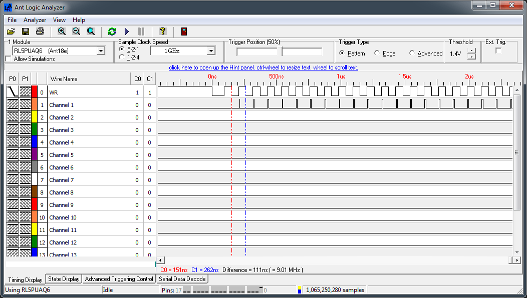
If you look closely you’ll see that the first cycle is slightly stretched compared to the others. I believe this extra clock cycle is being inserted by the MCU because the address for the str instruction is not yet set up on the bus but am not entirely sure (remember what I said about the fun involved with programming a pipelined architecture!).
Overclocking the controller
Yes you can. I did it several times by accident during the development of the Gpio16BitAccessMode template. My first attempt at the access mode resulted in a 42ns/42ns write cycle and it ran through my graphics library demo without any glitches or other artefacts. Try overclocking if you want, but be aware that even if it appears to be successful you could be storing up trouble for later on. It’s your risk to take.
Watch the video
Here’s a short video showing the FSMC access mode running on the F4 Discovery board. This demo is included with stm32plus, named hx8352a.
Using it on the Arduino Mega
With the Arduino Mega being a 5V device and this screen being 3.3V, some kind of adaptor is required. Luckily that’s exactly what I built in in this article. It was very simple for me to hook up this screen in 64K colour mode and port the stm32plus driver to the Arduino.
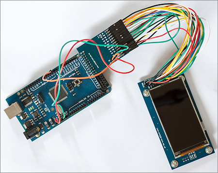
I’ve committed the driver code to the xmemtft github repository and created a release 3.0.1 that you can get from my downloads page. The highly optimised GPIO driver performs very well on this display. See for yourself in this youtube video.
Using the onboard SPI flash
The boards that I have built come with a Winbond W25Q16DW 16Mbit SPI flash IC and a breakout header to get at the functionality. The available pins on the breakout header are shown below.
| Pin | Function |
|---|---|
| SS | Slave select (active low chip-select). Pulled up to VDD. |
| HOLD | Hold input. Pulled up to VDD and can be left NC if not required. |
| WP | Write protect. Pulled up to VDD and can be left NC if not required. |
| MISO | MISO. Master in, slave out (data read from flash) |
| MISO | MOSO. Master out, slave in (data write to flash) |
stm32plus comes with two new example programs that exercise the SPI flash functionality. flash_spi_program is a general purpose programming utility that will program and verify a set of files that you supply on an SD card.
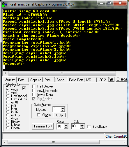
The above image shows the output of the flash_spi_program example when run against the sample files that I include with the example code.
The second example, flash_spi_reader, makes use of the example JPEG files programmed by the flash_spi_program example. It goes into a loop reading each image from the flash device and writing it to the KF700 LCD display.
Download the Gerbers
The Gerber files are now available from my downloads page. You can use them to get your own copies of the PCB printed at any of the popular online services.