


An Ethernet PHY for the STM32F107 and STM32F4
A what? If you’ve never crossed paths with ethernet technologies before then you may not know what an ethernet PHY is. Well, it’s the physical transceiver that converts a well-known data-bus protocol implemented by your MCU into the physical signals that go down the wire.
MCU ethernet support
MCUs such as the STM32F107 come with a degree of ethernet support built-in. The MCU provides a 10/100Mbs MAC and can talk the standard Media Independent Interface (MII) protocol to the outside world.
This is where the PHY comes in. The PHY receives the 4-bit wide MII protocol and synthesises the differential signals necessary to drive the ethernet RJ45 socket. It also does the reverse, decoding incoming signals from the RJ45 connector and talking MII back to the MCU.
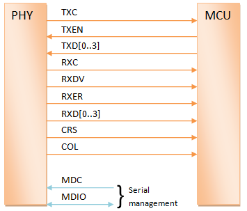
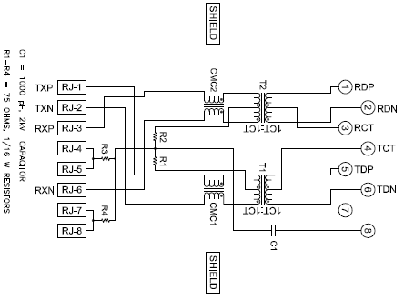
The MII protocol connections
This separation of concerns reduces overall cost by limiting the complexity of the components outside the MCU.
Other options
Only a minority of MCUs have ethernet support. The STM32F107 is one, the STM32F2 and STM32F4 series are others. Ethernet tends to feature in special series MCUs or newer and more expensive devices.
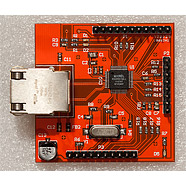
There’s an STM32F107 modestly hiding behind the faded print
If you don’t happen to have one of those then all is not lost. Companies such as Wiznet with their W5100 device have taken the logical step of integrating the MAC, PHY and the entire TCP stack into one IC. If you don’t have ethernet support on your MCU then this is what you could use, but it will cost a little more due to the increased feature set and the interface is likely to be serial which may limit performance.
Another option is to buy the ST official PHY add-on board for their F107 development board but it’s pricey, and it’s much more fun to build your own.
This article will focus on building a PHY targeted at the STM32F107 but compatible with any MCU that can talk the MII protocol.
The PHY IC
There’s a few of them to choose from, and they’re all much of a muchness, I mean how exciting can you make an ethernet 10/100 transceiver? ‘Not very’ is the answer to that question. They all implement the basic protocol and then add various extras such as indicator LEDs, error detection and various types of auto-detection of your configuration.
The one I selected is the Micrel KSZ8051MLL, available at the time of writing from Farnell in single units for 86p. Yes, 86 pence is all you need to fork out for the core IC in a PHY.
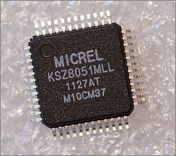
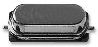
The KSZ8051MLL in LQFP48 7x7mm package, 0.5mm pitch.
Features of the KSZ8051MLL
Here’s a functional diagram of the KSZ8051MLL taken from the datasheet that shows how it fits into the ethernet physical layer.
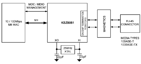
Functional diagram.
As well as providing the core PHY support the KSZ8051MLL has some useful extra features:
- Interrupt support so we don’t have to continually poll the device to find out when something has happened.
- LED outputs for link, speed and activity status.
- Auto detection of straight-through and crossover cables so you can use either type. (I like this one!).
- Power saving modes – ethernet is quite power-hungry when it’s active.
- Diagnostics for detecting where a cable fault lies, and diagnostics for detecting pin-to-board faults.
- Single 3.3V (or 2.5V or 1.8V) power input – the 1.2V regulator is built in.
- On-chip termination resistors for the differential pairs.
Bootstrapping
Upon power-up or hard reset the PHY has to configure its internal registers with some default values. Rather than hardcode some defaults, the device uses the rather ingenious method of momentarily sampling the levels (high or low) of a selection of its pins and using those levels to configure the registers.
That means that a low-cost board could configure the PHY by setting appropriate pull-ups and pull-downs on the pins and thereby not have to write microcontroller code to configure the device through software. Code not written is flash memory not used is money saved.
Well, we have a micrcontroller and rather a good one at that, so we’ll be configuring the registers to known values through software after a hard reset.
A development board schematic
After reading the datasheet, and the application notes on Micrel’s website, I decided that a development board should not be too hard to design. The challenges would lie in creating a reliable, interference free design that could cope with the high-frequency ethernet signals.
I took Micrel’s reference development board schematic as a starting point and modified it to remove features that I wasn’t going to need, and to adapt it so that it would work with the external components that I was going to select.
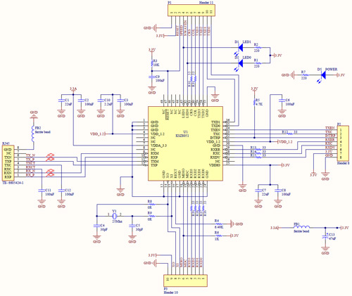
The schematic. It’s too large to read on this page so click the image to open it in a PDF
Basic design features
The design follows the recommendations made in the Micrel application note for the PHY with some modifications made by myself to tailor it for use by a powerful MCU such as the STM32F107.
There are no jumpers for setting the hardware strapping options. We will accept the defaults provided by the internal pull-ups and pull-downs on the PHY and make any adjustments via register access after reset. In practice the only limitation of this approach is that the PHY ID number will be fixed at ‘1’ because there is no writeable register available to reconfigure this after reset.
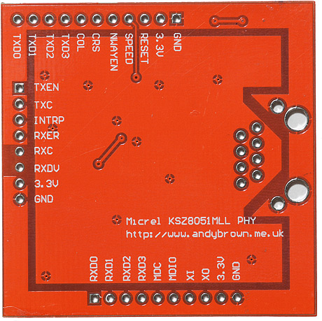
All the PHY lines except the differential pairs are exposed in 2.54mm pin headers arranged around the board.
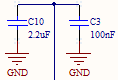 |
Decoupling of the power lines follows the advice in the application note and the datasheet, and we add 47µF of bulk capacitance to the board. Ferrite beads are used to suppress interference. |
 |
33Ω resistors are used on the MII signal lines to limit reflections. This design feature is also present in the Micrel reference design. The termination resistors that are commonly found between the differential TX/RX pairs and the PHY are not required in this design because they are integrated into the PHY itself. |
The RJ45 connector
Ethernet design guidelines state that there must be a 1:1 isolation transformer between the cable and the PHY. These are known as the magnetics.
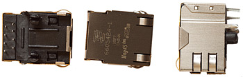
The TE Mag45 connector
Ethernet transformers are surprisingly expensive in small quantities so in my design I’ve chosen the TE 6605424-1 connector that integrates the magnetics and an ESD protection circuit into the connector.
The TE Mag45 schematic
RJ45 connectors that integrate the magnetics are commonly known as magjacks and are better value than buying the transformer and connector separately. Even so, this is the most expensive part in the design.
The clock
10/100 ethernet systems require a 25Mhz clock that runs at full speed for 100Mb/s operation and is internally divided down to 2.5Mhz when the link is set to 10Mb/s.
The 25Mhz crystal
The design allows for the 25Mhz clock to be sourced from an onboard crystal or from an external clock. In the former case R8 and R9 are solder bridges (or 0Ω resistors). In the latter case the clock should be applied to the XI pin and R8 and R9 are not connected.
I have chosen an Abracon ABLS-25.000MHZ-B2F-T crystal with an 18pF load capacitance requirement. The formula for choosing the values of the two load capacitors is well documented on the internet. It is:
C1 = C2 = 2 * CL - (CP + CI)
Where CP is the parasitic capacitance of the board and CI is the input capacitance of the PHY. For my Abracon crystal with its CL of 18pF this works out at C1 = C2 = 30pF, assuming the commonly quoted CP + CI = 6pF.
I’m a little concerned at the additional capacitance introduced by the presence of the XO and XI header pins. If the capacitance is too far from the ideal level then the crystal frequency will be off target or it may not even start oscillating.
I’ll be using my 1Ghz Ant18e logic analyser to check that the crystal’s output frequency is correct. I can measure the frequency at one of the PHY clock pins. Any attempt to measure it at the XI and XO pins will fail due to the the capacitance of the probes being added to the load capacitance seen by the crystal.
Bill of Materials
Here’s the full list of parts that I selected for this project. All of them are available from Farnell Electronics and I have included direct links to each part’s page at Farnell.
| Identifiers | Description | Mftr. & Part No. |
| C13 | CAPACITOR, CASE D, 47µF, 16V | PANASONIC – EEEFC1C470P |
| C2,C3,C6,C8,C9,C11,C12 | MLCC, 0603, Y5V, 50V, 100NF | MULTICOMP – MCCA000256 |
| C4,C5 | CAPACITOR, NP0, 0603, 50V, 30PF | KEMET – C0603C300J5GACTU |
| C10 | MLCC, 0603, X5R, 6.3V, 2.2µF | MULTICOMP – MCCA000516 |
| FB1,FB2 | FERRITE BEAD, 0603 CASE, 220Ω | MURATA BLM18PG221SN1D |
| P1,P2,P3 | HEADER, VERTICAL, 1ROW, 36WAY | TE CONNECTIVITY / AMP – 8-146274-6 |
| R3 | RESISTOR, ANTI SULPHUR, 0603, 10K | WELWYN – ASC0603-10KFT5 |
| R4 | RESISTOR, 0603, 6K49, 1% | VISHAY DRALORIC – CRCW06036K49FKEA |
| R5 | RESISTOR, 0603, 4K7 5%, 0.1W | PANASONIC – ERJ3GEYJ472V |
| R6 | RESISTOR, 0603, 1K 5%, 0.1W | PANASONIC – ERJ3GEYJ102V |
| U1 | TXRX, PHY, 10/100, MII, 3.3V, 48LQFP | MICREL SEMICONDUCTOR – KSZ8051MLL |
| R8,R9 | RESISTOR, 0Ω, 0R 0.1W | PANASONIC – ERJ3GEY0R00V |
| RJ45 | JACK, MAG45, THRU HOLE | TE CONNECTIVITY – 6605424-1 |
| Y1 | CRYSTAL, 25M, 18PF CL, HC49/4HSMX | ABRACON – ABLS-25.000MHZ-B2F-T |
| D1 | LED, YELLOW, 0603, SMD | KINGBRIGHT – KPT-1608YC |
| D2 | LED, GREEN, 0603, SMD | KINGBRIGHT – KPT-1608SGC |
| C1,C7 | CAPACITOR, X5R, 0805, 6.3V, 22µF | AVX – 08056D226MAT2A |
| R1,R2,R7 | RESISTOR, 0603, 220R 5%, 0.1W | PANASONIC – ERJ3GEYJ221V |
| D5 | LED, RED, 0603, SMD | KINGBRIGHT – KPT-1608SURCK |
| R10..R19 | RESISTOR, 0603, 33R 5%, 0.1W | PANASONIC – ERJ3GEYJ330V |
PCB layout
The CAD for the board didn’t take too long. A few component footprints had to be created from scratch and I always route by hand these days.
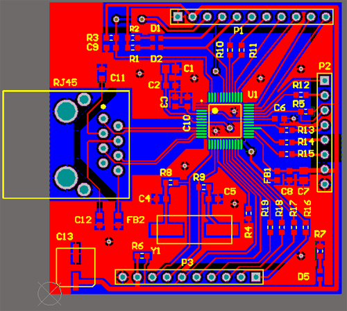
The board CAD layout with layers merged
I only wish I’d had space on the top layer where the header pins are to label each pin with its function. Doing so would have exceeded the 50mm square limit that I was working to.
After designing the CAD I exported the Gerber CAM files and uploaded them to ITead Studio for manufacturing. A couple of weeks later they arrived.
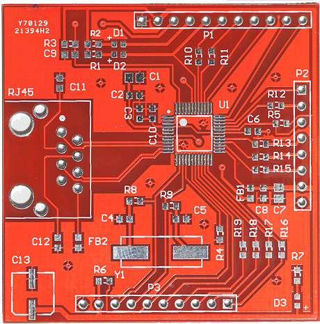
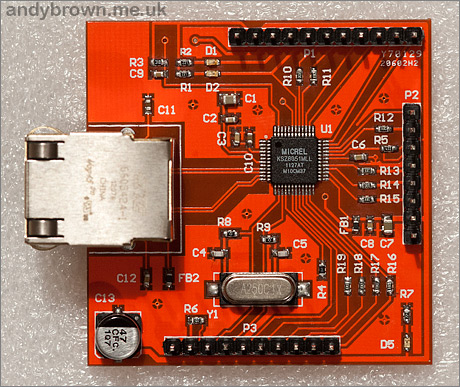
The front of the board, looks great in red!
The differential TX/RX pairs are clearly visible snaking from the PHY to the RJ45 connector. The +/- lines are kept close to each other and have their lengths equalised as much as possible. Other signals, including the top ground pour are kept well away from these traces to help minimise interference.
I don’t do ground pours as a matter of course, only if the design calls for it and in this case the Micrel notes recommend it. I have seen reports on the internet of issues with prototype board manufacturing and ground pours that come into close proximity with other signals so I set a conservative 15 mil pour-to-trace clearance and removed ‘islands’ (areas of the pour that are not connected to a signal).
The back of the board
The back of the board contains the chassis and signal ground planes. Chassis ground from the RJ45 socket is isolated from the large central signal ground plane by an isolation moat. The break in the moat over on the right is to prevent a loop antenna being created.
The fully built PCB
The build process was fairly straightforward. I followed my usual procedure of reflowing on a hot-plate for the IC and any parts that have concealed pins. That meant the 47µF capacitor and the crystal in this case. Both of those do have enough of their pins protruding to hand-solder them but the majority of the pins are underneath so reflow is preferred. Also, their bases are plastic and would easily melt if they came into contact with an iron or an over-enthusiastic hot-air gun.
After reflow the remaining discrete components were simply hot-air’d into place with a pair of fine tweezers. The majority are 0603 size which is the smallest size I can work with both quickly and accurately. I can (and do) work accurately with 0402, but not quickly! The last steps are to use an iron to solder the headers and finally the RJ45.
Testing
I decided that the first stage of testing would be to simply verify that the thing is alive. By alive, that means that the clock is active and the PHY is responding to commands. So, I powered it up and wrote a small STM32 program that exercised the built-in NAND tree self-test mode.
This test involves first setting all pins high then pulling each one low in sequence and checking another pin to ensure it toggles from low to high or high to low. The result of the test was…
Fail!
Nothing happened. The PHY appeared to be completely ignoring me. After much head-scratching I decided that the clock cannot have started so I got my multimeter out, set it to continuity testing mode and meticulously tested the pads on a blank board for continuity where it should be and none where it should not be.
Found it! On close inspection there is an unwanted connection between R9 and the ground pour. Furthermore as bad luck would have it the connection is very hard to see because it’s under the silkscreen label. It’s visible under the microscope though.
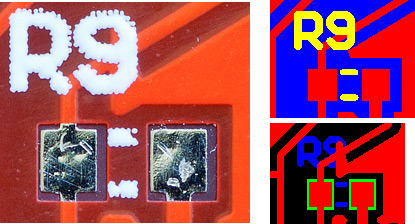
Bad Gerber!
At first I thought it was a manufacturing defect until, that is I checked everything in the chain and found that the Gerbers had been badly generated by the
I spent some time investigating the issue and it turned out to be an option in the Camtastic ‘Export Gerber’ dialog that was selected by default and should be deselected to avoid the bug:
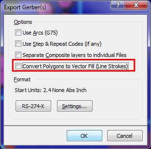
Deselect this checkbox
Deselecting the highlighted option results in Gerbers that appear to be correct, at least as far as I can tell by inspecting them in the Viewplot preview program.
Anyway, the fix for the boards that have already been manufactured involves the surgical application of a sharp knife to break the unwanted trace and I’m back in testing mode.
That did the trick. This time the NAND test passed with flying colours and I can move on to measure the clocks.
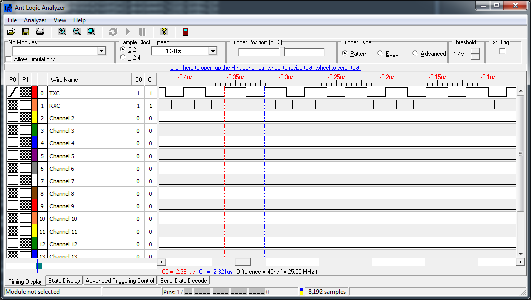
Clock testing with a logic analyser. Click for larger
The PHY outputs a clock on TXC and RXC when in MII mode and the line is disconnected. At 100Mb/s (the default) this clock will be the full 25Mhz. I set my logic analyser to its maximum asynchronous sampling rate of 1GHz and measured both pins. As you can see from the image above they are both spot on 25Mhz. Perfect.
Software driver
ST publish sample code that is designed to operate with their ST802RT1 PHY. It demonstrates a point-to-point web-server using the lwIP TCP stack.
The project is laid out in the same structural form as every other ST sample that I’ve seen. As much as I dislike flat, procedural ‘C’ code, there’s a lot to be said for the predictable format that ST uses. Once you’ve seen one then you’ll know exactly where to look in all the others.
The key changes that I needed to make to the sample were to change some preprocessor definitions for the status register and speed and duplex masks. Around about line 354 of stm32_eth.h I added:
//#define PHY_SR 31         /*!< Tranceiver Status Register */
/**
  * @brief  For DP83848
  */
//#define PHY_SR 16     /*!< Tranceiver Status Register */
/**
  * @brief  For Micrel KSZ8051MLL
  */
#define PHY_SR 0x1e     /*!< Tranceiver Status Register */
And slightly further on I added:
/**
  * @brief  For DP83848
  */
//#define PHY_Speed_Status  ((u16)0x0002)    /*!< Configured information of Speed: 10Mbps */
//#define PHY_Duplex_Status ((u16)0x0004)    /*!< Configured information of Duplex: Full-duplex */

/**
  * @brief  For Micrel KSZ8051MLL
  */
#define PHY_Speed_Status    ((u16)0x0001)    /*!< Configured information of Speed: 10Mbps */
#define PHY_Duplex_Status   ((u16)0x0004)    /*!< Configured information of Duplex: Full-duplex */
With these in place all I needed to do was comment out the stuff related to flashing LEDs via the HTTP server because I’m only interested in testing the link and the data transfer. The sample code compiled OK and I uploaded it to the MCU.
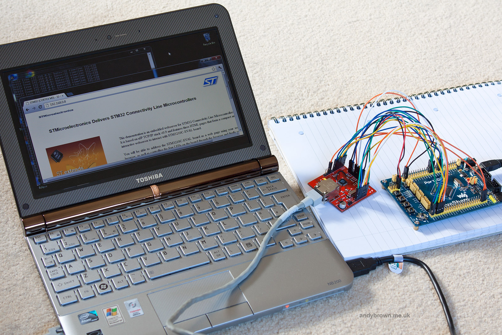
Embedded web server. Click for larger (600kB) image
It works! The link with the netbook is auto-negotiated at 100Mb/s full duplex. The embedded lwIP protocol stack, hardcoded to IPv4 address 192.168.0.8, is configured to respond to ICMP ping requests which you can see in the command prompt window. More impressively you can see Google Chrome successfully downloading a web page from the embedded http server.
Final testing
I decided to do a final round of testing to ensure that the design is robust. The aim was to verify all the possible link modes and ensure that there were no errors received on the line – too many framing errors could indicate a signal integrity problem due to interference.
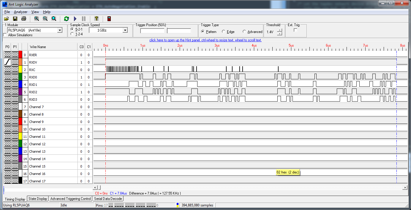
I hooked up my logic analyser to the RXDV, RXER, RXC and RXD[0..3] lines and took some samples triggered on the rising edge of RXDV (data valid) line. The results are shown in the image above. I also left it running for about 10 minutes with a trigger on the RXER line (receive error) while flooding the local network with broadcast UDP packets. It was never triggered, indicating that the signal integrity was perfect.
I tested the following configurations and all performed as expected:
- Auto-negotiation of speed and duplex
- 100Mb/s full and half-duplex
- 10Mb/s full and half-duplex
- Straight-through and crossover cables (auto MDI/MDI-X).
An stm32plus driver?
It’s here! I’m happy to say that the KSZ8051MLL is one of the supported PHYs in the all-new TCP/IP stack included with stm32plus 3.0.0. Click here to read all about it.
Print your own PCBs
Want to have a go at assembling one of these boards yourself but don’t have a home etching kit? No problem, just download the Gerbers from my downloads page and use a service such as that offered by ITead Studio, Seeed Studio or Elecrow.
Version 2 now released
I have produced a new version of this development board that uses the popular Hanrun HR911105A connector and has a few other incremental improvements. See this article for a complete write-up.
Pingback: interface ARM controller (say STM32F4) to Internet()