


512Kb SRAM expansion for the Arduino Mega (build)
The second in this series of articles covers the PCB design and build process for the memory expansion board
The Eagle board layout
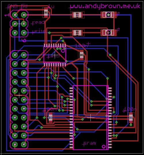
The board layout
The signal lines are 10mil wide and the power lines are 16mil. I hand routed some of the power lines myself and then let Eagle’s much-maligned auto-router do the rest. After experimenting with some different placements and orientations of the ICs I managed to get the number of vias down to an acceptable number – too many vias is an indication that you may be able to make some improvements by repositioning the ICs.
Parts list
| Part | Number | Package | Quantity |
|---|---|---|---|
| SRAM | Alliance AS7C4096A 12ns | 44 pin TSOP-II | 1 |
| Latch | NXP 74AHC373 | 20 pin TSSOP-20 | 1 |
| Capacitor | 100nF | 0603 | 3 |
| Capacitor | 1µF | 0603 | 1 |
| Resistor | approx 430Ω | 0805 | 2 |
| LED – yellow | Kingbright | 1206 | 1 |
| LED – red | Kingbright | 1206 | 1 |
| Jumper | 2 pins | 2.54mm | 2 |
| Male DIP header | 22 pins | 2.54mm | 1 |
| Male DIP header | 6 pins | 2.54mm | 1 |
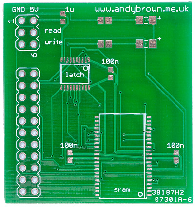
The PCB
I use the prototype PCB manufacturing service offered by ITead Studio. If your board is double sided and comes in at under 50mm square then they will charge US$9.95 for 10 copies including delivery.
Mine comes in at around 40x43mm so no problems there. ITead supply a DRC file that you can use to validate your design against their equipment. The finest trace/space they can handle is 6mil but in my opinion you’d be asking for manufacturing faults at that level so I try to stick to 10mil or higher.
The only downside of ordering from China like this is that the delivery time to the UK is about 2 weeks.
The bare PCB
Soldering SMD parts
If you google around the internet you’ll find a few articles dedicated to explaining how you can hand-solder SMD parts. The method that I use is to pre-tin all the solder pads with a normal iron and then fix the parts by reflowing the solder with a hot air gun. I use regular solder (not paste) and smelly, messy but very effective rosin flux when working with the regular iron and no-clean liquid flux when working with the hot air gun.
The secret to success here is to use an absolutely tiny amount of solder on each pad when tinning so the pad goes from flat to a tiny bump. If you create too much of a solder bump then multi-pin parts will not sit down evenly and you’ll have to manually fix them up afterwards with a fine-tip iron and a microscope.
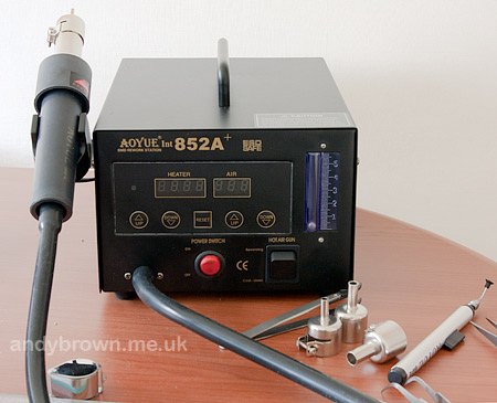
The Aoyue 852A+ hot air rework station
Although the hot air station makes working with SMD parts quite simple I think in future I’ll set a minimum size of 0805 for the discrete parts because 0603 is just too fiddly to work with.
After soldering I inspect each joint with a 20x binocular (stereo) microscope and resolve any dry joints with the finest tip soldering iron that I have.
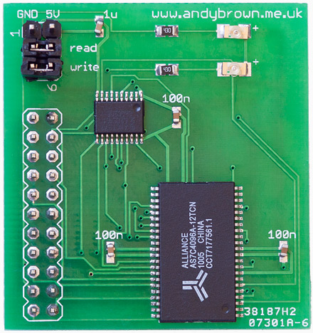
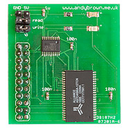
The finished PCB
The finished PCB is designed to press directly into the Arduino Mega connectors without blocking off any more pins than it uses. Finally here’s a picture of the daughterboard attached to the Arduino Mega 1280. The GND and 5V supply pins are not connected in this image.
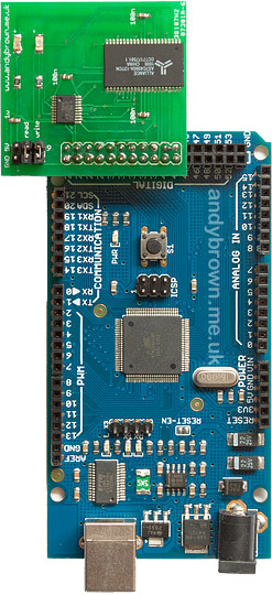
Attached to the Arduino
Other articles in this series
| 512Kb SRAM expansion for the Arduino Mega (design) |
| 512Kb SRAM expansion for the Arduino Mega (software) |
Schematics, PCB CAD and Gerbers
I don’t have any more boards left to sell, but you can now print and build your own by downloading the package from my downloads page. Good luck!