Tags
Related Posts
Share This


Project Difficulty
- All components are commonly available.
- The smallest IC pin pitch is 0.5mm
- The smallest discrete component is 0603.
- All components are on the top-side of the board
- The 8MHz oscillator has pads that are under the package
Recent Posts
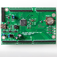
A development board for an STM32G081 MCU
I’ve been an avid user of ST’s F0 series ever since it was launched. The 48MHz Cortex M0 is almost always the perfect MCU for every project that I tend to build and it’s so easy to program and debug that, for me, it’s the default answer to ‘which MCU should I use for this project?’ So when I noticed that ST had launched a ‘G0’ range I just had to have a closer look.
What’s the difference?
In short, there’s a Cortex M0+ core at the heart of the G0 series instead of the M0 that’s in the F0. To find out the difference between the M0 and the plus we have to visit ARM’s website.
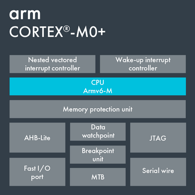
Cortex M0+ block diagram
There’s a slight increase in performance and an optional Memory Protection Unit (MPU) that the RTOS guys may get excited about but really there’s not much else in the way of additional features.
The headline claim made by ARM is a further decrease in the already class-leading power consumption and a scarcely concealed attack on the remaining market for 8-bit MCUs. ARM really want you to choose this core for projects that might previously have used an 8-bit device.
A shorter pipeline
One interesting way that they’ve managed to decrease power consumption is by reducing the number of clocks required for the instruction pipeline from three to two by squashing the instruction decode stage across the two clocks and reducing the need for power-expensive access to flash memory.
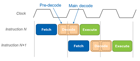
Pipeline clocks and stages
I have to say that I’m not convinced that this is a good thing for performance. The marketing blurb correctly states that a shorter pipeline increases responsiveness but we engineers will immediately point out that faster response means lower throughput. High-end devices such as the Intel i7 have more than 20 pipeline stages and even ARM’s own Cortex-M7 has 6 stages.
However, ST have given us more features that I think will make the G0 series the default choice for my future designs.
F0 vs G0
Clock speed. You can’t fail to notice that the maximum clock speed for the G0 is 64MHz compared to 48MHz for the F0. The cynic in me says that this is compensation for the performance hit incurred by shorter instruction pipeline.
Flash memory. The F0 goes up to 256k. ST has plans for the G0 to go up to 512k but so far they’ve only released the G071 and G081 that go up 128kb.
SRAM. The F0 goes up to 32k. The G0 improves slightly on that with 36k. More SRAM is always good so that’s a welcome improvement.
Price. They’re about the same. If I compare the STM32F091RBT6 to the similarly spec’d STM32G081RBT6 then they come about about the same with the G0 edging it with the 36k SRAM and 64MHz maximum clock.
ST’s development boards
At the time of writing ST are offering two development boards. There’s the low cost G071 Nucleo that features a degree of Arduino compatibility though goodness knows why they bother with that.
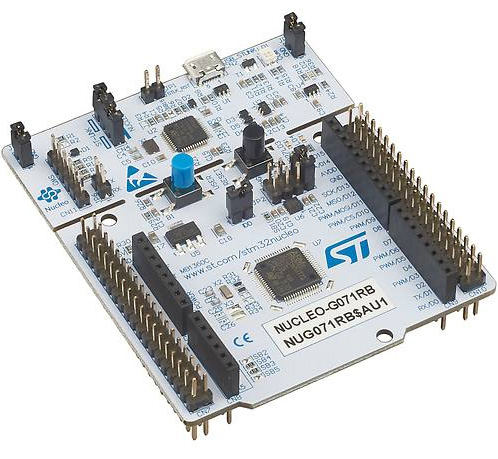
The G071 nucleo board
At just $10 the Nucleo is really cheap and a great way to kick the tyres of the G0 series if you want to get started really quickly.
The other board on offer is a full-featured eval board featuring the STM32G081RBT6 MCU and costing an eye-watering $400.
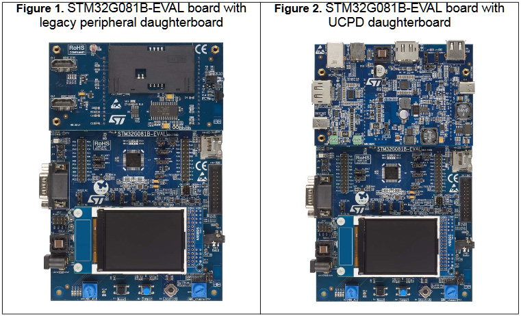
The G081 eval board
To be fair, for that $400 you do get a ton of peripherals to play with. If your employer is paying then this might be the board you want to buy.
I almost bought a Nucleo board but then reconsidered and decided that the best way for me to learn about the ins and outs of the G0 would be to build my own development board. So that’s what I did.
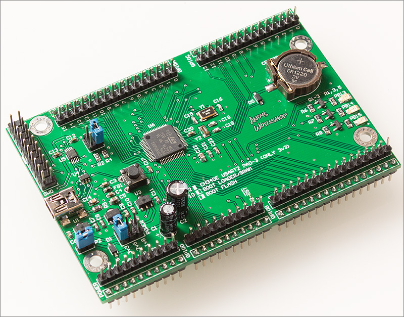
My development board design
I decided that I’d go for the following features on my board.
- STM32G081RBT6 MCU with 128k/36k flash/SRAM in the LQFP-64 package.
- All GPIO pins to be available on top pin headers, grouped by port and ordered by pin.
- All pins also to be available in breadboard-friendly 100mil spaced headers on the bottom of the board.
- Three selectable power supplies: 3.3v, 2.5v and 1.8v.
- Three user LEDs routed to ports that have timer outputs available so flash/fade effects can be protyped.
- A third-party USB-to-serial IC will connect an MCU USART to the outside world through a mini-USB port.
- External 8MHz HSE oscillator so that the USB-to-serial IC can be used at high speeds.
- External LSE 32.768kHz oscillator for RTC use with backup coin-cell battery.
The STM32G081RBT6 was selected because it’s currently the biggest one that ST have released and it always helps to have the most resources available on your dev board.
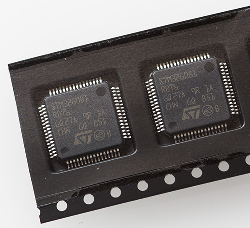
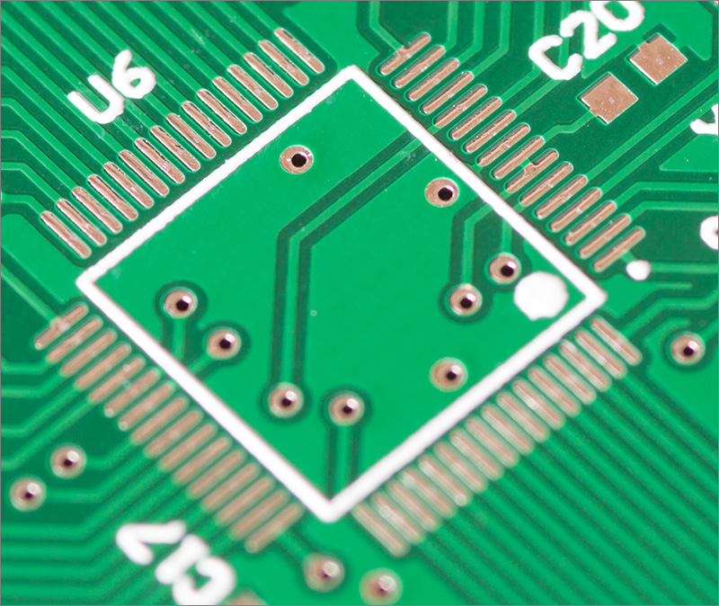
The 64-pin G081 IC
When it comes to transferring your design from the dev board to a custom PCB then that’s when you can downsize to a device optimised for your resource usage.
I decided right away that the pin headers would expose every GPIO port and pin group and the headers would be grouped by port and ordered by pin. I’m seriously bored with hunting for pins on development boards that have been ordered to facilitate easy PCB routing!
Pin headers will be provided on the top and bottom of the board, just like the ST Discovery boards except mine will have pins on top that are long enough to actually accept a jumper wire without them falling off because they’re too loose.
A selectable power supply has always been something I’ve wanted from a development board. If my project is standalone then I’ll probably run it at 3.3v but there are times when I need something else. For example interfacing with an FPGA might require 2.5v and a battery-powered design might be spec’d to run at 1.8v to optimise power consumption.
A standalone IOT device might be required to keep accurate time so I decided to include a 32.768kHz LSE oscillator and the associated backup battery. This will be a 3v CR1220 coin-cell.
It’s quite common for an MCU to have to connect back to something more powerful such as a PC or Raspberry PI so I’ve included a USB-to-serial device – the cheapo CH340E – on my board. To enable driving the CH340E at high data rates I’ve included an 8MHz HSE oscillator so that the MCU peripheral clocks will be as accurate as they can be.
The CH340 saga
I’ll start with a confession. This is my second attempt at building this board. The first attempt was largely the same as the second except that first time I used the CH340G instead of the CH340E. And the CH340G didn’t work.
The CH340/341 series are a family of USB to serial converters that fulfil the same role as the much more well known FTDI chip that you can find on official Arduino boards. The CH340 is made by a Chinese company, WCH, and is much cheaper than the FTDI chip. I bought my CH340’s for about £3 for 10 on Ali Express. The internet says good things about the CH340 so I felt confident.
The CH340 is actually a series of ICs that come in different packages that provide different levels of functionality. The datasheet is all in Chinese but has been translated to English and can be found here.
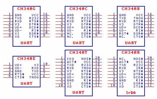
All the CH340s (so far)
The 340G is the first one that I bought, and it arrived in packaging that I would not describe as confidence-inspiring.
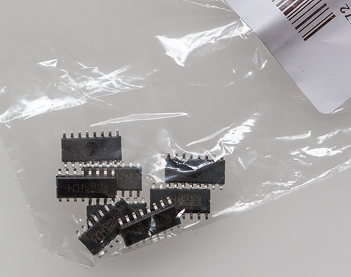
Loose packed ICs
Nevertheless I made a board with it and selected a good quality Abracon surface mount 12MHz oscillator to support it. Unfortunately it would not enumerate as a USB device. I think it was having trouble getting the oscillator to start as I couldn’t detect a signal coming from it and I’m fairly sure my probes weren’t loading the crystal down as I could probe another, similar oscillator on the board. On power up I could see short spurious waveforms come from the oscillator but they never stabilised and the output always went flat.
I tried higher load-capacitors, then lower. Then a new CH340G. Nothing worked and I was out of options so I decided to cut my losses, and my time, and replace the CH340G with the CH340E that has a built-in oscillator and requires only decoupling capacitors to use it. I could of course have switched to an FTDI but that would be giving up and I wasn’t ready to do that. Unfortunately the IC package was different so I also had to redesign that part of the board.
Three weeks later and the new boards arrived and so have the new ICs, again from Ali Express. This time though the packaging was much more like they’d actually come from a production reel and not some trader’s back pocket.
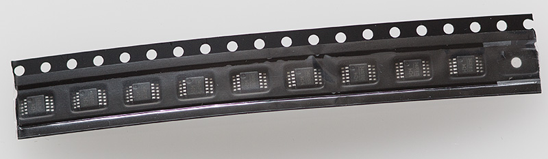
Proper IC packaging
We’ll see how I get on later in this article, but now let’s have a look at the schematic for the development board.
Schematic
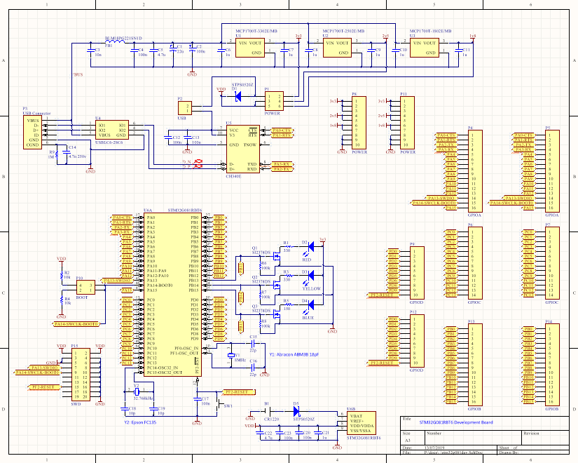
Schematic image
Click on the full image to see a PDF of the schematic. It’s quite a modular design so let’s break it down into its parts.
The power supplies and the USB interface
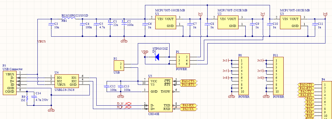
I wanted to have a choice here and linear regulators are cheap so I designed in three of them to give power supply options of 3.3v, 2.5v and 1.8v. A jumper is provided to select the desired level. Since the power input comes from the potentially very noisy 5V USB line I’ve included my usual filter network consisting of a ferrite bead and some capacitors.
The USB interface is provided by a mini-B connector. I only ever use the mini-B or the full size B connector on my boards because they’re the most reliable. The micro-B connector used by most smartphones before they started switching to type-C is too delicate and easy to tear off the board. The on-board components are protected from static by the USBLC6 IC that I include as a matter of course with every USB design.
The CH340E can only run at 3.3v and can be enabled with the P2 jumper. D1 ensures that when 2.5v or 1.8v are selected then that level does end up being routed to the VCC pin of the CH340. The voltage drop of that same diode also has the effect of making VDD for the MCU actually about 3.0 to 3.1v instead of 3.3v. Something to be aware of.
The CH340E only requires a pair of decoupling capacitors to run at 3.3v, one on the VCC pin and the other on the V3 pin. The use of the diode D1 actually means that the CH340E will be powered at 3.3v and the signal levels will be about 3.0v but that’s within spec so I don’t expect any issues.
The STM32G081RBT6 MCU
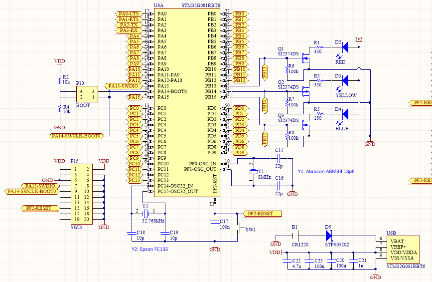
Here’s the heart of the system, the MCU. All the GPIOs are broken out to pin headers Except those that have crystals attached, though I don’t think those are any great loss to a designer.
External 8MHz and 32.768kHz surface mount crystal oscillators are provided as the HSE and LSE clock sources. There’s a reset button and the SWD programming interface is broken out to the ungainly 20 pin ARM connector that connects directly to my ST-Link programmer via the ribbon cable.
Three LEDs are provided that source current from the 3.3v supply regardless of the selected core voltage so that the brightness won’t vary — and in the case of the blue LED so it will actually light at all — when the supply is 1.8v.
ST have optimised the pins on the G0 series so that you get more GPIOs. In their older chips you’d find a pair of VDD/GND pins on each side of the package which I think tells you a bit about the internal floor planning of the device and how things are arranged internally on the die. This G0, however has a single VDD/VDDA pin and a single GND pin. VREF is there but they’ve done the decent thing and placed it right next to VDD/VDDA so you can tie them together and right next to those is VBAT, which obviously has to be separate.
I’ve designed in a coin-cell holder for a CR1220 3v backup battery, protected from reverse-current by a schottky diode with a low forward voltage. According to ST’s datasheet the worst-case current consumption for VBAT when VDD = 3.0v is 470nA. A quick look at Energizer’s datasheet shows that you can expect to get about 30mAh from it before the voltage starts to drop off. 0.00047mA into 30mAh gives 63829 hours or 7 years. I’m sure there are other losses and inefficiences to consider but still, that’s a long time.
IO connectors
They’re all there with the exception of those used by oscillators. One of the great things about ST’s package redesign is that there are now more GPIO pins available. GPIO ports A, B and C are fully available although in my design PC14 and PC15 are taken by the 32.768kHz LSE. This is great for designs that might need to bit-bang a parallel bus. GPIO port D has pins 0 to 9 available.
Bill of materials
Here’s the full bill of materials for this project.
| Identifier | Value | Quantity | Description | Footprint | Comment |
|---|---|---|---|---|---|
| B1 | 1 | CR1220 holder | Custom | available on ebay | |
| C1 | 22µ | 1 | Polarized Capacitor (Radial) | CAPPR2-5x11 | |
| C2 | 100µ | 1 | Polarized Capacitor (Radial) | CAPPR2-5x11 | |
| C3 | 10n | 1 | Capacitor | 0603 | |
| C4, C12, C13, C17, C20, C23 | 100n | 6 | Capacitor | 0603 | |
| C5, C22 | 4.7µ | 2 | Capacitor | 0805 | |
| C6, C7, C8, C9, C10, C11, C21 | 1µ | 7 | Capacitor | 0603 | |
| C14 | 4.7n 250v | 1 | Capacitor | 0805 | |
| C15, C16 | 22p | 2 | Capacitor | 0603 | |
| C18, C19 | 10p | 2 | Capacitor | 0603 | |
| D1, D5 | STPS0520Z | 2 | Schottky Rectifier | SOD123 | |
| D2 | 1 | LED | 2012 | RED | |
| D3 | 1 | LED | 2012 | YELLOW | |
| D4 | 1 | LED | 2012 | BLUE | |
| FB1 | BLM18PG221SN1D | 1 | Ferrite bead | 0603 | |
| P1 | 1 | Header, 3-Pin, Dual row | HDR2X3 | POWER | |
| P2 | 1 | Header, 2-Pin | HDR1X2 | CH340 EN | |
| P3 | 1 | USB Mini B | USB Connector | ||
| P4, P5 | 2 | Header, 16-Pin | HDR1X16 | GPIOA | |
| P6, P7 | 2 | Header, 14-Pin | HDR1X14 | GPIOC | |
| P8, P11 | 2 | Header, 10-Pin | HDR1X10 | POWER | |
| P9, P12 | 2 | Header, 10-Pin | HDR1X10 | GPIOD | |
| P10 | 1 | Header, 2-Pin, Dual row | HDR2X2 | BOOT | |
| P13, P14 | 2 | Header, 16-Pin | HDR1X16 | GPIOB | |
| P15 | 1 | Header, 10-Pin, Dual row | HDR2X10 | SWD | |
| Q1, Q2, Q3 | SI2374DS | 3 | MOSFET-N | SOT23-3N | |
| R1, R3 | 330 | 2 | Resistor | 0805 | |
| R2, R4 | 10k | 2 | Resistor | 0805 | |
| R5 | 150 | 1 | Resistor | 0805 | |
| R6, R7, R8 | 100k | 3 | Resistor | 0805 | |
| R9 | 1M | 1 | Resistor | 0805 | |
| SW1 | 1 | Button | PCB Button | RESET button | |
| U1 | MCP1700T-3302E/MB | 1 | SOT-89-MB3_N | LDO, 3-Pin SOT-89 | |
| U2 | MCP1700T-2502E/MB | 1 | SOT-89-MB3_N | LDO, 3-Pin SOT-89 | |
| U3 | MCP1700T-1802E/MB | 1 | SOT-89-MB3_N | LDO, 3-Pin SOT-89 | |
| U4 | USBLC6-2SC6 | 1 | SOT23-6_L | ||
| U5 | CH340E | 1 | MSOP-UN10_N | ||
| U6 | STM32G081RBT6 | 1 | ARM Cortex-M0+ | STM-LQFP64_L | |
| Y1 | ABRACON ABM3B | 1 | 8MHz crystal | Custom | |
| Y2 | Epson FC-135 | 1 | 32.768kHz crystal | 2012 |
PCB layout
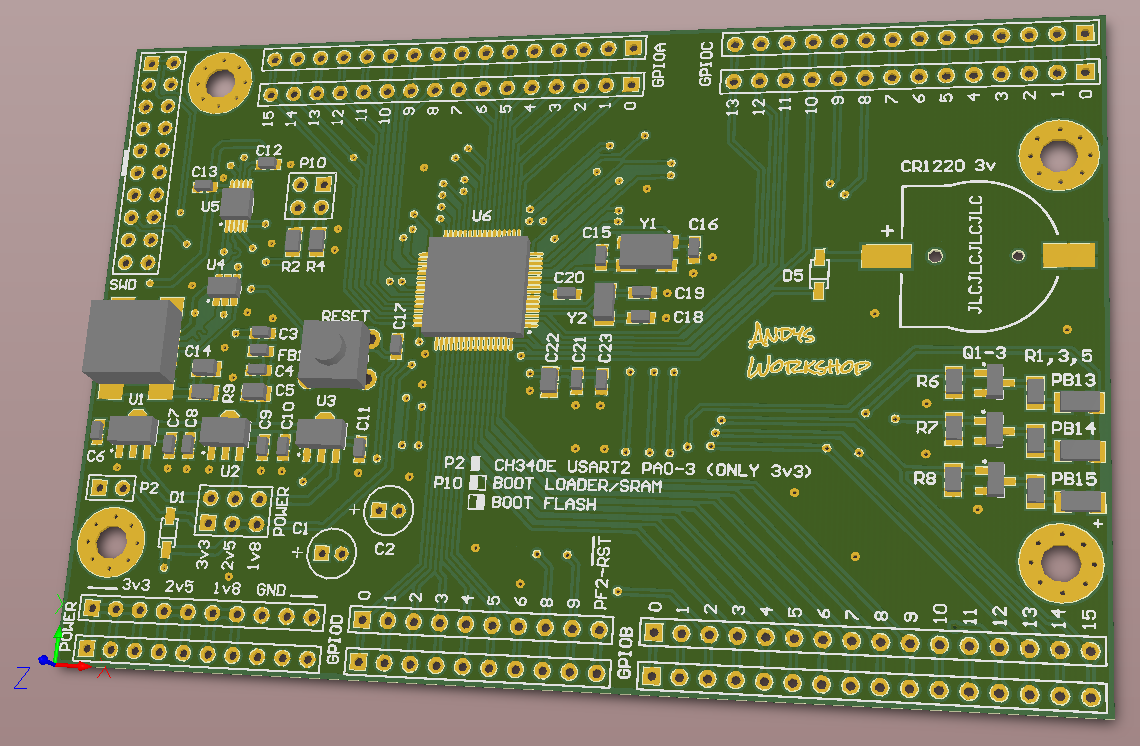
3D view of the board
The physical layout of the board is optimised for ease of use. I’m tired of boards that lazily route the GPIOs to the headers based on where they are on the IC package making me hunt up and down the tiny and often faded silkscreen legend for the right pin. On this board the GPIOs are grouped by port and ordered by pin number. It only takes a few extra seconds of routing time, even with ST’s knack of placing a port’s pins at seemingly random locations around the package.
I’ve provided rows of downward and upward facing pins for each port. The downward facing pins are designed to be the standard 100 mil apart all down the board and the rows on the opposite side of the board are a multiple of 100 mil away so that the board will mate with a breadboard.
The upward-facing pins are designed to accept the usual jumper wire-interconnects that we use so often.
Overall the board was easily routed on two layers with a ground plane top and bottom and is a little larger than ST’s discovery boards. I even had space for four M3 screw holes if the board ever needs to be permanently mounted into a chassis.
I uploaded the boards to JLPCB in China and paid the ridiculously low fee of $2 for a pack of 5. The lowest price shipping option added about $7 shipping to the price. Delivery took about 3 weeks.
Building the board
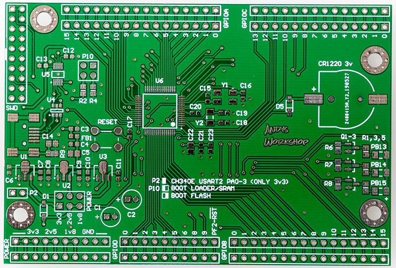
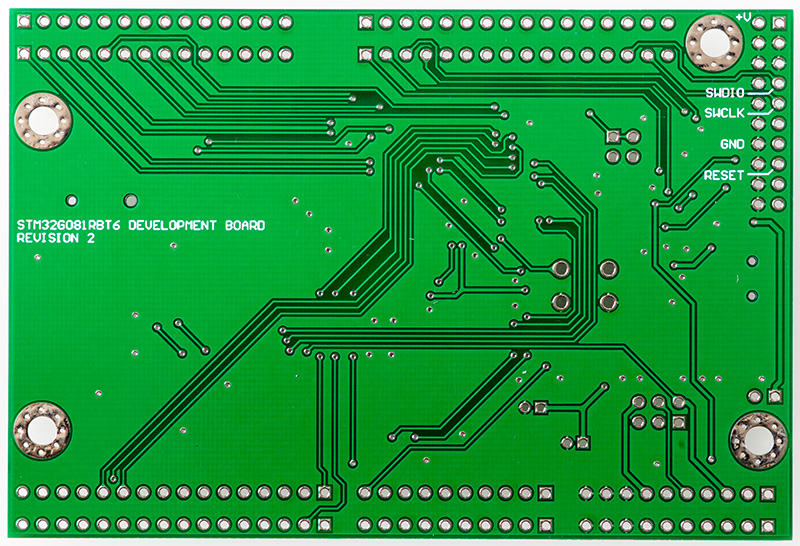
Top and bottom view of the bare board
The boards arrived and are looking great. I was particularly pleased to see that JLPCB have ignored the solder mask expansion around the pads. Solder mask expansion is the gap between the edge of a pad and where solder mask starts and is used to counter inaccurate placement of the solder mask in the manufacturing process.
Accurate solder mask placement
I set a rule of 4 mil which would leave a tiny solder mask sliver of about 1 mil between the MCU pins. It appears that JLPCB have enough confidence in their process to ignore the expansion rules and place the mask right up to the pins. The benefit of this is that I’ve got, as you can see above, a complete mask between the 0.5mm pitch pins of the MCU and that will greatly reduce the chance of accidental solder bridges.
My process for building a board is quite slow but I find it reliable. I first tin the pads with solder, then I reapply flux to the pads, then I place the surface mount components on the tinned pads and then I reflow the board in my halogen reflow oven. When the reflow is complete I touch up any problems manually and then solder in the through-hole components by hand. Finally I wash the board using hot soapy water and a toothbrush, rinse it off with cold water and leave it out to dry for at least a day.
All built and ready for testing
The reflow went OK this time. The only issue was that one of the 0603 capacitors got blown off its pads by the oven fan before it could reflow. I fixed that manually with my hot air gun.
One interesting thing I noticed while inspecting the board under my microscope was the design of the 32.768kHz crystal package.
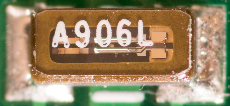
It took a 2x macro and many megapixels to shoot this
It appears that the designers wanted to show off the internals so they fitted a clear plastic window into the top of the 1206 package so you can see how it works. I have no idea how crystals are constructed but I do find it fascinating and it looks a bit like a tuning fork. Does anyone out there know what’s going on in there?
Testing the board
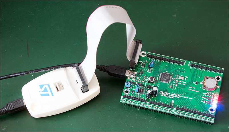
ST-Link hooked up to the board
With the first revision of this board giving me so many CH340-related problems I was naturally a little apprehensive when connecting this for the first time.
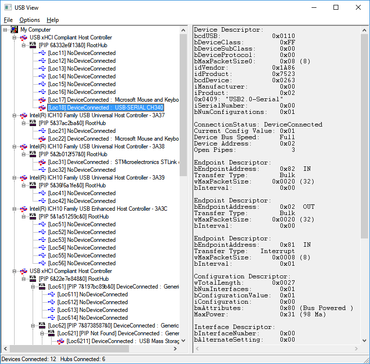
USB View looking good
I need not have worried, the CH340E enumerated first time, showing up immediately there in the Windows USB View utility. I could proceed with firmware testing.
I decided that the quickest way to test out the board would be to use ST’s STM32CubeMX software to auto-generate some code that would set up USART2 to talk to the CH340E and also the three pins that are connected to the LEDs.
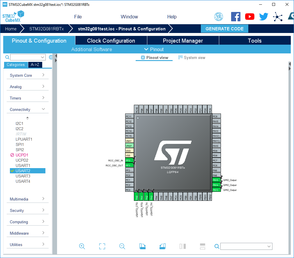
CubeMX pin configuration
I decided to enable RTS and CTS for USART operation even though I was going to operate in asynchronous mode for this test. I clicked through the CubeMX screens to enable the core clock at 64MHz using the external HSE as a clock source and then got it to generate a project for the free System Workbench for STM32 IDE. I’m pleased to see that this is yet another Eclipse-based IDE and I’ve been an Eclipse user for more than 15 years so I immediately feel at home and ready to code.
/* USER CODE BEGIN Header */
/**
******************************************************************************
* @file : main.c
* @brief : Main program body
******************************************************************************
* @attention
*
* <h2><center>© Copyright (c) 2019 STMicroelectronics.
* All rights reserved.</center></h2>
*
* This software component is licensed by ST under BSD 3-Clause license,
* the "License"; You may not use this file except in compliance with the
* License. You may obtain a copy of the License at:
* opensource.org/licenses/BSD-3-Clause
*
******************************************************************************
*/
/* USER CODE END Header */
/* Includes ------------------------------------------------------------------*/
#include "main.h"
/* Private includes ----------------------------------------------------------*/
/* USER CODE BEGIN Includes */
/* USER CODE END Includes */
/* Private typedef -----------------------------------------------------------*/
/* USER CODE BEGIN PTD */
/* USER CODE END PTD */Auto-generated code
ST’s auto-generated code isn’t too bad at all. I’ve seen all types of auto-generated code that range in quality from ‘that compiles?’ to some that really look like a human wrote it. ST’s code contains comments that mark out where you can place your code without fear of it being overwitten by re-runs of CubeMX when you need to change your design. That’s great but my advice would be to keep your modifications of auto-generated files to a minimum and always check in or stage your changes before you re-run CubeMX.
  /* USER CODE BEGIN WHILE */
  while (1)
  {
    /* USER CODE END WHILE */

    /* USER CODE BEGIN 3 */

    HAL_GPIO_TogglePin(GPIOB, GPIO_PIN_13);
    HAL_Delay(200);
    HAL_GPIO_TogglePin(GPIOB, GPIO_PIN_14);
    HAL_Delay(200);
    HAL_GPIO_TogglePin(GPIOB, GPIO_PIN_15);
    HAL_Delay(200);

    HAL_UART_Transmit(&huart2, (uint8_t *) "hello world\r\n", 13, 1000);
    HAL_Delay(400);
  }
  /* USER CODE END 3 */
My small additions to test the firmware
I added a few lines of test code to write out Hello World every second to the USART at 115200kbps and also cycle the LEDs. Compilation was immediately successful and the firmware was uploaded through the IDE’s connection to ST-Link via OpenOCD.
That CH340 again…
The firmware started running and the LEDs were cycling as expected but Windows was now having problems detecting the CH340E. What the? It was working before. Had I broken it? I fired up USB View and found it there with a different vendor ID than it had before.
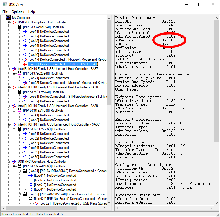
USB View showing the unexpected VID
When I first plugged in the board it had a VID of 1A86 which matches the VID in the Windows driver package that I downloaded. Now it’s got a VID of 9986 that doesn’t match anything in the driver. Weird.
My first reaction was to modify the driver package to include 9986 in the .INF file and re-install it. This worked so I was half pleased and half uneasy about what had actually happened. I decided to do some more research and it turns out that if the RTS pin ‘has too much load resistance’ at boot time then the CH340E will enumerate with a VID of 9986. This behaviour is undocumented (thanks for that) and my guess is that it’s a bootstrap configuration feature designed for a specific customer.
One solution is to not configure RTS if you’re not going to use it, or if you are then wait until USB enumeration is complete before you configure the pin and keep your fingers crossed that the CH340E doesn’t reset independently of the MCU. Another solution is to configure your drivers to accept both possible VIDs. That’s what I’ve done with Windows.
With my VID driver hack still in place I fired up Realterm, my favoured serial port test utility and configured it with the correct virtual port number and configuration. It immediately started ticking away with the expected Hello World message every second.
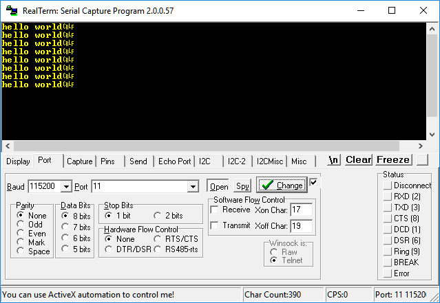
Realterm receiving data from the board
That’s a relief. Now I’m pleased that it all seems to work and I can go on to develop actual projects using the STM32 G0 series confident in the knowledge that they’ll work as expected.
Free gerber files
If you’d like to build this board yourself then you can download the Gerber files from here. They should be accepted by your favourite online PCB manufacturer.
Video and conclusion
If you’d like to watch a video of me faffing about with the PCB, explaining badly how it works and then stumbling through the firmware testing then it’s here on YouTube.
Embedding a video in the webpage looks cool but really you want to go to YouTube to watch it for the full high definition experience.
If you’d like to comment on this article then please leave a comment below or click here to visit the forum thread that I’ve started if you’d like to have a more lengthy conversation.