


Reverse engineering a server CPU voltage regulator module
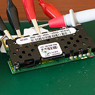
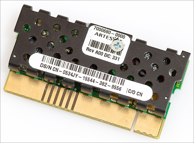
A recent ebay fishing expedition yielded an interesting little part for the very reasonable sum of about five pounds. It’s a voltage regulator module from a Dell PowerEdge 6650 Xeon server.
I originally bought this because I had the idea of salvaging parts from it to use in another project. These are high quality modules that will have very good inductors and sometimes an array of high value ceramic capacitors that could be re-used (ceramics of at least 22µF at 16V and above are rather pricey at the moment). So the VRM arrived and I was rather impressed with the build quality and decided to have a go at reverse engineering it.
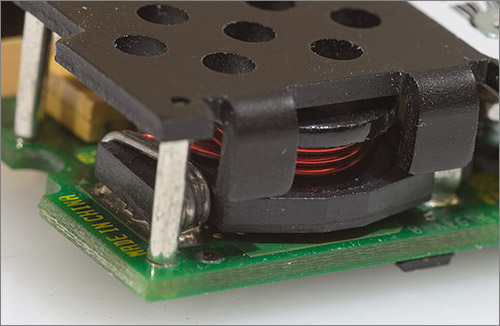
First impressions
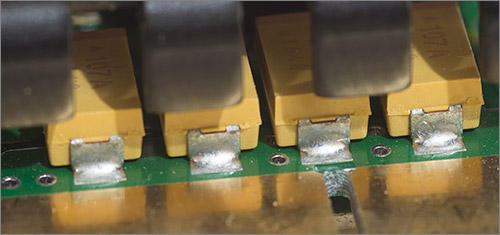
The board is at least 2 layers and I’m betting that the topology is a switching buck converter. If I peek under that big heatsink I can see a large inductor, a smaller inductor, Fairchild FDP7030L and FDB7030L power MOSFETs, a bank of ceramic and a bank of tantalum capacitors. Basically all the components you need for the power section of a buck converter. The inductors are Coiltronics UP2B-R47 and UP4B-1R5, both with maximum current ratings in excess of 10A. There’s also a MIC4420BM MOSFET driver with a peak current rating of 6A which gives us a clue as to the output current limit of this board.
The FDP7030L power MOSFET is screwed to the heatsink so I thought it’d be easy to get the heatsink off by just removing that screw. Not so. There are a number of ‘posts’ that prop the heasink up into position and I just couldn’t get these to budge without risking damage to the part.
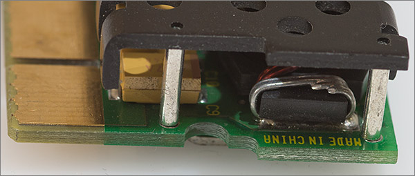
They’re soldered to the board and fixed somehow to the heatsink. My attempts at desoldering failed probably due to the heat that I applied being wicked straight up the post into the heatsink itself. I don’t want to damage this board so I’m afraid you’ll have to make do with some shots from around the sides where I can see under the heatsink.
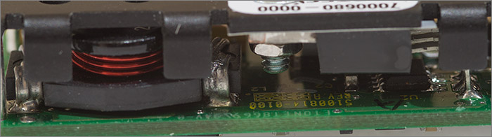
The control circuitry
Here’s where it gets interesting. There’s rather a lot happening on the control side of the board.

Click for larger
The big obvious 20 pin IC is an Intersil HIP6004B and sure enough the datasheet confirms that it is indeed a switching buck regulator with recommended applications that include the power supply for older generation CPUs.

Click for PDF
What makes this part interesting is the way that you select the output voltage. These days the typical method for setting the output voltage is to use a resistor divider but this device does it through a 5-bit digital input that feeds an onboard DAC.
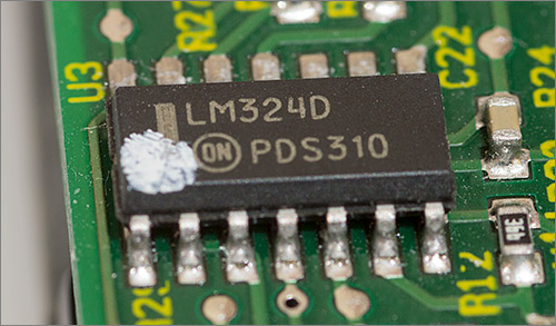
The other IC up the top left is an LM324D quad op-amp. I honestly cannot think what that’s doing on here and my searching around to find example applications that include such an op-amp array in this configuration yielded nothing. Maybe I’ll be able to figure it out during testing.
There are a large number of test pads dotted around the board but unfortunately none of them are labelled with the expected value.
Reverse engineering the power connections
My aim is to power this VRM up using a bench power supply and then to probe the various parts to find out what’s what. To do that I need to locate the power input and ground. I don’t need to locate the power output because I can probe for that but I think it’ll be an easy one to guess anyway.
Firstly, let’s locate ground. Here’s the pinout of the IC.
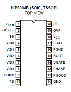
Ground is on pin 11. I set my meter to the continuity testing buzzer and probed around the golden fingers. Easy. All the fat fingers on the heatsink side are ground. No worries.
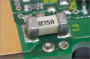
Let’s move on to VCC, the power input. It’s on pin 18 and a big obvious hint on the control circuitry side is the presence of a white SMD fuse down at the bottom right. The ‘LF’ logo is Littlefuse and it’s rated at 15A.
Yes, that was it. The fat finger on the right is the power input. I could go ahead and power it up right now and probe for the power output but let’s see if it’s where I think it is.
Switching regulators like this one have an inductor in series with the output voltage so all I need to do is probe either pin of that big inductor under the heatsink and the suspect fat fingers on the control side that are unaccounted for.
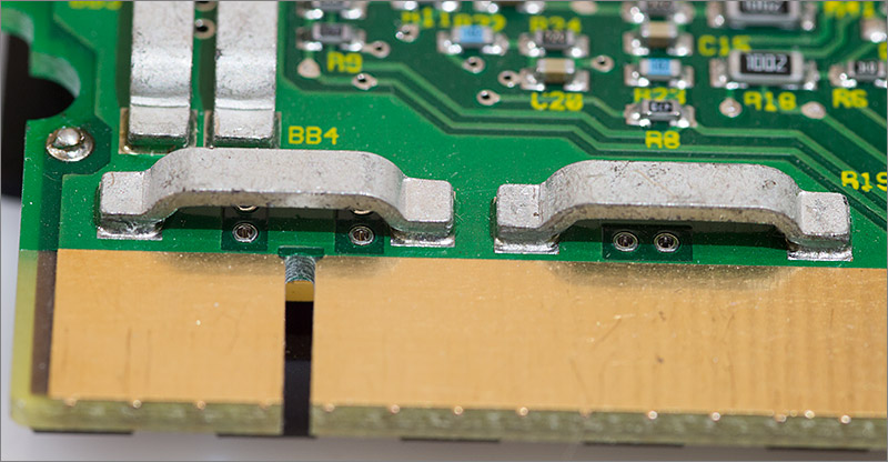
Sure enough those pins confirm to be the power output. Those metal bars are interesting aren’t they? Each one of them bridges over some vias in a large copper fill. The silk screen label prefix of ‘BB’ probably stands for ‘bus bar’ which is a common engineering term for a big fat conductor. I assume that the designers were trying to ensure that the current delivery is as even as possible across all the golden fingers. It’s certainly an interesting design decision and does hint at a belt-and-braces design.
Now I can power it up and see what it actually does.
Power on
I rigged up my bench power supply to the board using crocodile clips to clamp to the power and ground connections. Wads of paper are used on the ‘other’ side of the crocodile clips to prevent unwanted short circuits.
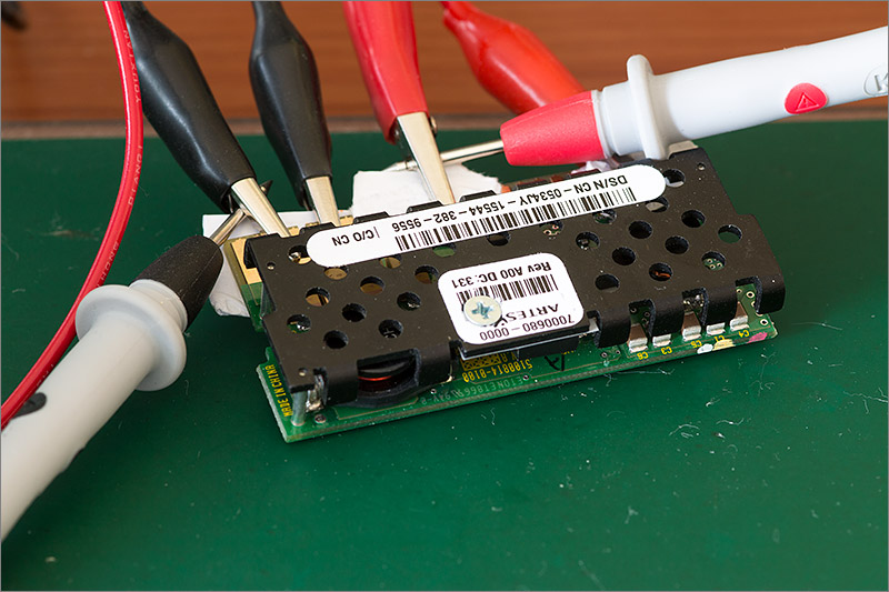
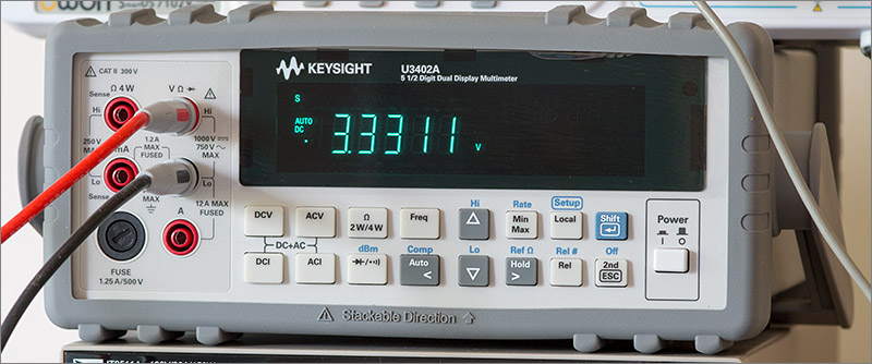
The Intersil IC claims to operate at 5V and 12V, both of which are present on a computer motherboard so I dialled in the lower 5V value and powered up. I probed the power output to see what was there. Nothing. OK, time to try 12V. This time I got a much better result. 3.3V and change was present on the output pins.
That’s a really useful output voltage for hobby use. I had a quick probe around the pins of the Intersil IC with an oscilloscope to see if I could locate a waveform that would give away the switching frequency. There it was on pin 13, the PHASE pin.
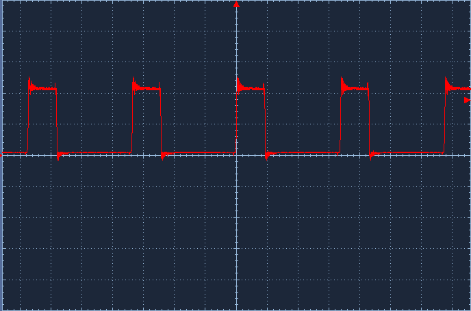
The frequency of that PWM waveform is 296.3kHz with an amplitude of 12V.
What I need to do now is set up a test rig to see how stable the output is under load, and the best way to achieve that is to use a piece of test equipment called a DC Electronic Load.
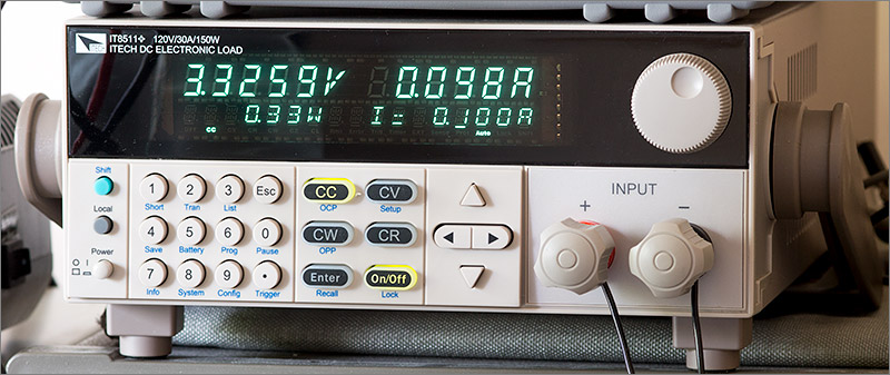
These devices apply a load to a circuit under test. You’ll get some combination of constant current, voltage and power modes depending on how much you want to spend. The maximum wattage is also a price differentiator. I got this Itech IT8511+ on Ali Express. Itech are the OEM for BK precision loads so you know that this is a quality part.
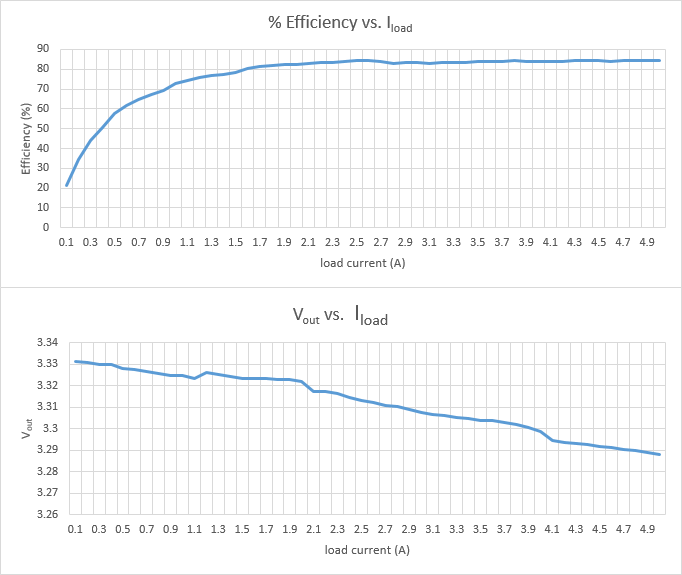
I’ll test this circuit in constant current mode. That means I dial in a current on the load and the device will sink up to that current while burning it off as heat. My bench power supply is limited to 3A output but if you recall your basic physics you’ll remember that power is conserved throughout the system so if I put in 1A at 12V and get 12W then a perfect power supply would deliver 12W / 3.3V = 3.6A at the output.
In reality the power supply is far from perfect and some of those 12 watts will be lost. Typical efficiencies for switching power supplies range from 70 to over 90% depending on a number of variables including the load current.
I ran the test and applied a gradually increasing load up to 5A. I stopped there, not because it was getting hot – it wasn’t, the heatsink was just warm but because I know the MOSFET driver is rated at a maximum of 6A and there may be other, lower rated components that I don’t know about.
I have an accurate Keysight U3402A bench multimeter so I decided to take a number of readings at steadily increasing intervals of 100mA from zero to 5A to see how stable the output was and also to calculate the efficiency percentages.
| I-load | I-in | P-in | Vout | Pout | Ploss | Efficiency |
|---|---|---|---|---|---|---|
| 0 | 0.11 | 1.32 | 3.3321 | 0 | 1.32 | 0 |
| 0.1 | 0.13 | 1.56 | 3.3313 | 0.33313 | 1.22687 | 21.35448718 |
| 0.2 | 0.16 | 1.92 | 3.3307 | 0.66614 | 1.25386 | 34.69479167 |
| 0.3 | 0.19 | 2.28 | 3.3298 | 0.99894 | 1.28106 | 43.81315789 |
| 0.4 | 0.22 | 2.64 | 3.3298 | 1.33192 | 1.30808 | 50.45151515 |
| 0.5 | 0.24 | 2.88 | 3.3282 | 1.6641 | 1.2159 | 57.78125 |
| 0.6 | 0.27 | 3.24 | 3.3276 | 1.99656 | 1.24344 | 61.62222222 |
| 0.7 | 0.3 | 3.6 | 3.3269 | 2.32883 | 1.27117 | 64.68972222 |
| 0.8 | 0.33 | 3.96 | 3.3258 | 2.66064 | 1.29936 | 67.18787879 |
| 0.9 | 0.36 | 4.32 | 3.3249 | 2.99241 | 1.32759 | 69.26875 |
| 1 | 0.38 | 4.56 | 3.3247 | 3.3247 | 1.2353 | 72.91008772 |
| 1.1 | 0.41 | 4.92 | 3.3235 | 3.65585 | 1.26415 | 74.30589431 |
| 1.2 | 0.44 | 5.28 | 3.3263 | 3.99156 | 1.28844 | 75.59772727 |
| 1.3 | 0.47 | 5.64 | 3.3253 | 4.32289 | 1.31711 | 76.64698582 |
| 1.4 | 0.5 | 6 | 3.3244 | 4.65416 | 1.34584 | 77.56933333 |
| 1.5 | 0.53 | 6.36 | 3.3236 | 4.9854 | 1.3746 | 78.38679245 |
| 1.6 | 0.55 | 6.6 | 3.3233 | 5.31728 | 1.28272 | 80.56484848 |
| 1.7 | 0.58 | 6.96 | 3.3234 | 5.64978 | 1.31022 | 81.175 |
| 1.8 | 0.61 | 7.32 | 3.323 | 5.9814 | 1.3386 | 81.71311475 |
| 1.9 | 0.64 | 7.68 | 3.323 | 6.3137 | 1.3663 | 82.20963542 |
| 2 | 0.67 | 8.04 | 3.322 | 6.644 | 1.396 | 82.63681592 |
| 2.1 | 0.7 | 8.4 | 3.3174 | 6.96654 | 1.43346 | 82.935 |
| 2.2 | 0.73 | 8.76 | 3.3174 | 7.29828 | 1.46172 | 83.31369863 |
| 2.3 | 0.76 | 9.12 | 3.3165 | 7.62795 | 1.49205 | 83.63980263 |
| 2.4 | 0.79 | 9.48 | 3.3146 | 7.95504 | 1.52496 | 83.91392405 |
| 2.5 | 0.82 | 9.84 | 3.3132 | 8.283 | 1.557 | 84.17682927 |
| 2.6 | 0.85 | 10.2 | 3.3122 | 8.61172 | 1.58828 | 84.42862745 |
| 2.7 | 0.89 | 10.68 | 3.3108 | 8.93916 | 1.74084 | 83.7 |
| 2.8 | 0.93 | 11.16 | 3.3103 | 9.26884 | 1.89116 | 83.05412186 |
| 2.9 | 0.96 | 11.52 | 3.309 | 9.5961 | 1.9239 | 83.29947917 |
| 3 | 0.99 | 11.88 | 3.3077 | 9.9231 | 1.9569 | 83.52777778 |
| 3.1 | 1.03 | 12.36 | 3.3066 | 10.25046 | 2.10954 | 82.93252427 |
| 3.2 | 1.06 | 12.72 | 3.306 | 10.5792 | 2.1408 | 83.16981132 |
| 3.3 | 1.09 | 13.08 | 3.3053 | 10.90749 | 2.17251 | 83.39059633 |
| 3.4 | 1.12 | 13.44 | 3.3048 | 11.23632 | 2.20368 | 83.60357143 |
| 3.5 | 1.15 | 13.8 | 3.3041 | 11.56435 | 2.23565 | 83.79963768 |
| 3.6 | 1.18 | 14.16 | 3.3038 | 11.89368 | 2.26632 | 83.99491525 |
| 3.7 | 1.21 | 14.52 | 3.3031 | 12.22147 | 2.29853 | 84.16990358 |
| 3.8 | 1.24 | 14.88 | 3.3021 | 12.54798 | 2.33202 | 84.32782258 |
| 3.9 | 1.28 | 15.36 | 3.3005 | 12.87195 | 2.48805 | 83.80175781 |
| 4 | 1.31 | 15.72 | 3.2987 | 13.1948 | 2.5252 | 83.93638677 |
| 4.1 | 1.34 | 16.08 | 3.2945 | 13.50745 | 2.57255 | 84.00155473 |
| 4.2 | 1.37 | 16.44 | 3.2938 | 13.83396 | 2.60604 | 84.14817518 |
| 4.3 | 1.4 | 16.8 | 3.293 | 14.1599 | 2.6401 | 84.28511905 |
| 4.4 | 1.43 | 17.16 | 3.2925 | 14.487 | 2.673 | 84.42307692 |
| 4.5 | 1.46 | 17.52 | 3.2918 | 14.8131 | 2.7069 | 84.54965753 |
| 4.6 | 1.5 | 18 | 3.2911 | 15.13906 | 2.86094 | 84.10588889 |
| 4.7 | 1.53 | 18.36 | 3.2902 | 15.46394 | 2.89606 | 84.22625272 |
| 4.8 | 1.56 | 18.72 | 3.29 | 15.792 | 2.928 | 84.35897436 |
| 4.9 | 1.59 | 19.08 | 3.2888 | 16.11512 | 2.96488 | 84.46079665 |
| 5 | 1.62 | 19.44 | 3.288 | 16.44 | 3 | 84.56790123 |
While collecting the data I noticed how the output voltage behaved at each level. The output voltage typically fluctuated by 500µV or so except around 1.8 to 2A where the fluctuations were more like 1 or 2mV. As the output voltage approached 3.3000V it appeared to become much more stable, often sitting without any fluctuation at all on my meter.
The data in the table can be visualised in these charts.
Analysing the rest of the board
It’s great that I can use the board as a 3.3V power supply as-is, but it would be really nice if I knew what the little golden fingers on the edge connector did. To help with this I photographed and printed out both sides of the PCB.
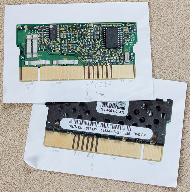
Having it down on a piece of paper really helps because you can jot down notes directly onto the image as you discover things. On the PCB side I labelled the little fingers A through F. Here’s what I managed to find out about them.
| A | B | C | D | E | F |
|---|---|---|---|---|---|
| 3.3V | NC | 12V | PGOOD | 12V | NC |
The 3.3V and 12V outputs are a mystery to me. They snake off through many components in the direction of the op-amp and the values don’t seem to change with load.
PGOOD is an easy one. That’s an open-drain output from the Intersil IC that floats when everything’s fine and is driven to ground when it’s not. Apply a pullup resistor to your MCU’s IO supply to sense the output of this pin.
I did the same sort of thing on the heatsink side, labelling the pins G through K. Here’s what I could find out.
| G | H | I | J | K |
|---|---|---|---|---|
| NC | NC | input | NC | input |
Only two of the contacts are actually connected to anything. I probed them and found that they weren’t driven to any particular level so I measured the resistance to ground and found it to be more or less exactly 50Ω which would appear to make them input pins.
I guessed that perhaps these pins formed part of an external resistor-divider that might calibrate the output voltage so I tried applying various resistances to ground, to the output voltage and using a potentiometer to create a divider. The good news was that there was some response from the output voltage as I experimented, but only ever upwards. That is, all I could do was cause the output voltage to rise slightly, nothing I did caused it to fall which wasn’t much use.
Video
I put together a video on YouTube of me fumbling around trying to figure this thing out. Click below or better still browse to the YouTube site to watch it in glorious high definition.
Summary
It’s a tale of two halves really. I’m pleased that I’ve managed to power up the board and get a useful output voltage from it but I’m a little disappointed that I could not identify what most of the IO pins on the board are doing. I could easily mount one of these into an edge connector and build a little power supply around it, and I may yet do that. However I’m going to hold off for a while to see if anyone out there has any tips regarding the unknown functionality of the unknown contacts. Please leave a comment down below or visit the forum thread and post your suggestions there.
Update: breakthrough!
Thanks to some excellent work by a blog reader the Artesyn (as opposed to Dell) part number has been identified. It is an NXA66 and the datasheet is available with the complete pinout documented in it. Click here to download the datasheet.
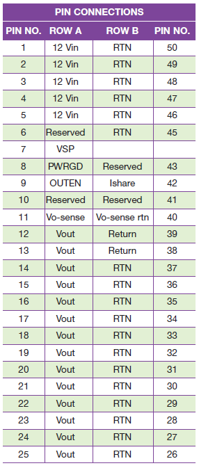
Here’s a snapshot of the pinout table from the datasheet. This is very good news. I’ve already got some 2×25 2.54mm edge connectors so I can now go ahead and design a cheap little PSU board around this high quality module. More to follow in due course.