Tags
Related Posts
Share This


Project Difficulty

Recent Posts
Old, not obsolete. Working with the Xilinx Virtex-E FPGA in a huge BGA package.
Let me see now, it must have been about two years ago when this story started. I was bored. I can’t remember why but when I’m bored I often surf ebay just to see what interesting bits and pieces are out there. Mostly it’s the same old stuff repeated over and over. Cheap bare PCB modules from the far east at the low end and chancers wanting $1000 for a broken oscilloscope at the other.
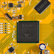
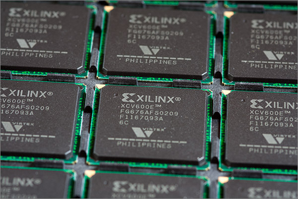
This time though I found something interesting. Someone in Sweden was selling a job lot of forty factory-sealed Virtex-E FPGAs for what amounted to two quid each. And they were big ones — the XCV600E-6FG676. ‘Virtex’ is Xilinx-speak for ‘expensive’, just look at the asking price for any of the current Virtex FPGAs to get an idea of the pricing and make sure you’re sitting down first. Now the Virtex-E is far from current, in fact Xilinx have marked it as obsolete but it’s still one big bad FPGA loaded to the gills with resources and now it seems that we hobbyists can get our hands on them.
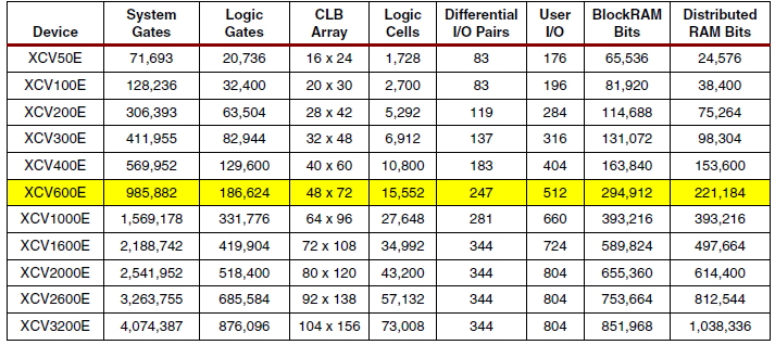
Those are big specs for an FPGA but the drawback is the package. It’s a BGA. Probably the hardest package for a hobbyist to work with and this is a massive 676 ball version.
I didn’t have the tools to work with these things. I didn’t care. I bought them anyway.
The present day
Fast forward to today and all forty are still in their waffle tray in my parts drawer (sound familiar?). But now times have changed. I have a halogen reflow oven capable of near-perfect reflow profile tracking and the Chinese prototype PCB manufacturers can produce four layer boards with 6/6mil tolerance that can be pushed to 5/5mil. I think it’s time to see what I can do with these FPGAs.
Logic. Lots of logic
The general aim of this project will be to create a generic development board for the FPGA. This isn’t as simple as it is for a microcontroller because an FPGA can become pretty much anything you want it to be and the resulting support circuitry is always tailored to the desired use case. In my case I’ll narrow the field down a little by focussing on I/O and interfaces to external memory devices.
I’ll aim to break out as many of the single-ended and differential I/Os as possible and hope to provide connectivity to some SRAM, SDRAM and flash memory. With that in mind, I need to take a look at this package to see what I’m up against.
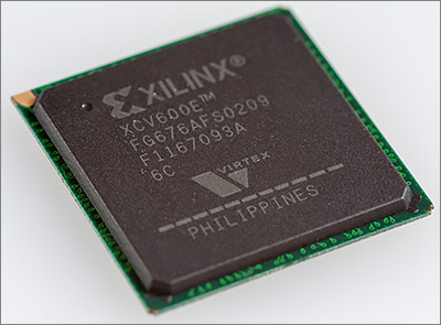
The Virtex-E is an early BGA design. You can see from the top view that the plastic package that holds the die is bonded to a PCB at the base — you can just see the green PCB surface peeking out from the edges. Let’s take a look at the bottom.
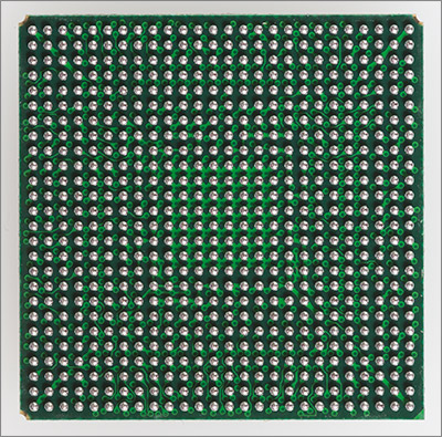
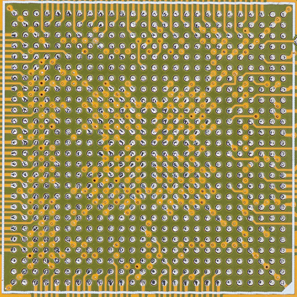
Quite the fascinating sight, that. 676 little solder balls arranged in a 1mm grid. Let’s take a closer look at the PCB that the balls are attached to.
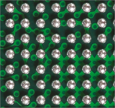
You can clearly see the fine traces that link the die to the ball pads on the PCB. The traces are terminated with teardrop shapes to give a more durable connection to the pads. Let’s look at the technical challenges involved with working with this package and see what I can do to mitigate them.
Escape routing
The first issue is escape routing the balls. Escape routing is the process of routing out traces from between the balls to the PCB at large. The size of the traces and vias that you can use depends on the pitch of the ball grid. Thankfully Xilinx publish XAPP157 which explains the recommended design parameters for complete escape routing of the FG676 package.
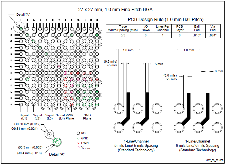
The only problem with the design rules in that table is the requirement for six layers. The cheap Chinese prototyping houses cannot yet do six layer boards at a hobby-friendly price. You’re looking at a few hundred pounds for a pack of ten compared to about fifty pounds for a four layer pack. I’ll just have to work with four layers and not route out all the pads. The chances are that I won’t have board space to route them all out anyway.
Further in the document Xilinx even give a suggested escape routing strategy for each layer.
The two missing layers from the diagram are the solid ground and split power planes. Even though I’m not going with a six layer design I’ll still use this as a guide for establishing patterns used to route out adjacent balls.
Reflow
Another advantage of these older BGA packages is that they’re not lead-free. If you’re looking at a Xilinx BGA device code then the ‘FG’ part of the name means leaded and ‘FGG’ would mean ‘lead free’. Leaded balls melt at an appreciably lower temperature than lead-free which means that I stand a better chance of success in my reflow oven because higher temperatures mean that the risk of damage to components increases.
I’ve managed to convince myself that I can deal with this package and create a development board for it so it’s time to come up with a schematic.
Development board schematic
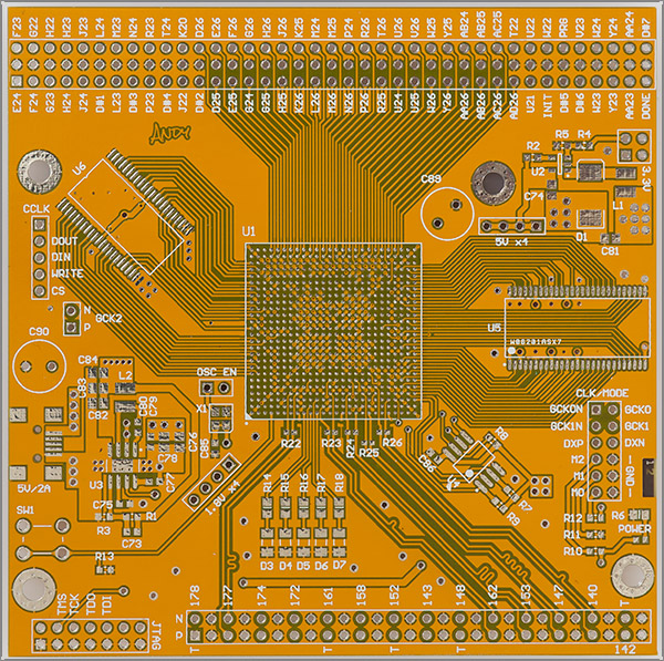
Here’s the full schematic and it’s a big one. Click on the thumbnail to download a PDF.
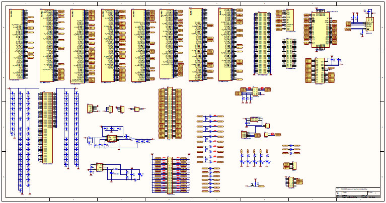
Let’s take a look at each section of the schematic in more detail.
The FPGA banks
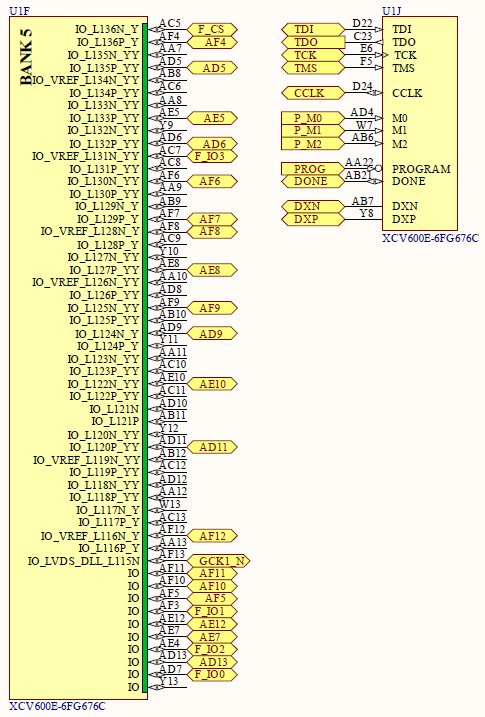
The XCV600E is so big that it’s split up into logical sections on the schematic. Most obvious are each of the banks of logic. Inside an FPGA the fabric is divided into separate banks of related logic, each with its own power supply and voltage reference inputs and all the banks are interconnected by high speed routing logic and low-skew clock distribution nets.
Missing from these older FPGAs are hard logic blocks such as multipliers, DSP functionality and differential serialisers. If you need those then you have to create them out of the fabric. Newer FPGAs tend to feature all of these and more which makes it easier to get a new design off the ground with some basic building blocks created from hard logic.
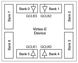
The diagram from the datasheet also shows where the global clocks (GCLKs) enter into the device. It’s expected that the global clocks will be high-fanout nets — that is, pretty much every one of your HDL processes will receive a signal from a GCLK or some derivation of it. Therefore these nets are designed to reach all banks in the device with very low skew. Clock skew in an FPGA can lead to metastability bugs which must rank amongst the hardest class of bugs to find.
I’ve selected I/Os to expose on the development board based on several factors. All I/Os with an alternate function are exposed such as JTAG and other programming methods as well as all the clocks. As many differential pairs as I can are exposed along with as many GPIO I/Os as I can route on the four layer board.
Clocks
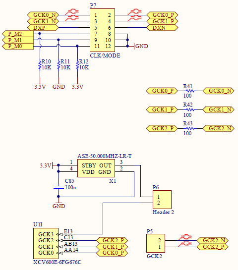
There are four GCLKs on the XCV600E and all of them can be either single ended or differential. I’ve exposed GCLK0, 1 and 2 as pin headers and provided 100Ω parallel termination for the differential pairs. GCLK3 is connected to a 50MHz on-board oscillator that provides a single-ended CMOS 50MHz signal on the positive GCLK3 I/O. This signal can be disabled by removing the jumper on P6.
The Virtex-E has eight on-board delay locked loops (DLLs). These allow a GCLK to be doubled or divided by 1.5, 2, 2.5, 3, 4, 5, 8, or 16.
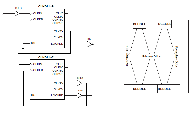
In addition to that, one DLL can be linked to another to yield a 4x multipler. It was with this in mind that I selected the 50MHz on board clock. With the doubling, linking and all those dividers I can reach a lot of useful frequencies. These DLLs are not as powerful as the Digital Clock Manager (DCM) in the Spartan FPGAs but there are a lot of them on board and the combination of doublers, dividers and chaining allow good flexibility.
Power supply scheme
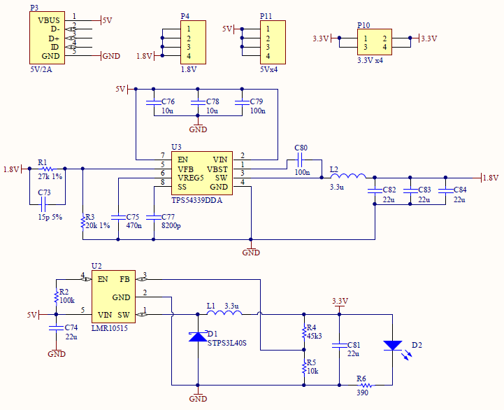
By now I’m used to FPGAs being a pain in the power supply department and the Virtex-E is no exception. I want to power my board from the now ubiquitous USB connector. Low power designs can be powered directly from a computer port and high power designs from one of those 2A wall chargers. The Virtex-E needs two supplies which makes it less of a pain than the Spartan 3 but it makes up for that in the demands that it can make on the current.
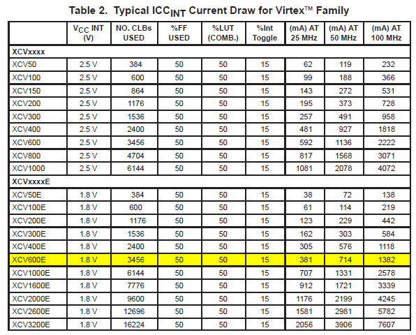
The core supply (VCCINT) required by the Virtex-E family is 1.8V which improves on the 2.5V required by the normal Virtex by reducing power consumption and therefore the heat dissipation. I googled a bit and discoverd SLVA086, a paper from TI that gives typical expected VCCINT power consumption for a fairly heavily loaded design. 1.4A was their worst-case.
Clearly I’d need a switching buck regulator to cover this worst case and the part that I selected was a TI TPS54339DDA. This part can handle up to 3A but the limiting component in my design is the inductor on the output that has a 2.1A DC saturation current.
The other supply required by the FPGA is the supply to the I/O buffers (VCCIO) and this one is typically selected to match the requirements of the external peripherals that you’ll need to talk to. I’ve selected 3.3V as the VCCIO level and, referring back to TI’s helpful analysis I can see that the current demands are, as you might expect, very much lower.
Despite the low demands I’m going with a switcher again. This time it’s one that I’ve used many times before, the LMR10515, again from TI. This is another one that requires few external components and is very simple to use. If you ever need a simple switcher that can drop 5V down to 3.3, 2.8 or any of the other common core supply voltages then I can highly recommend this one.
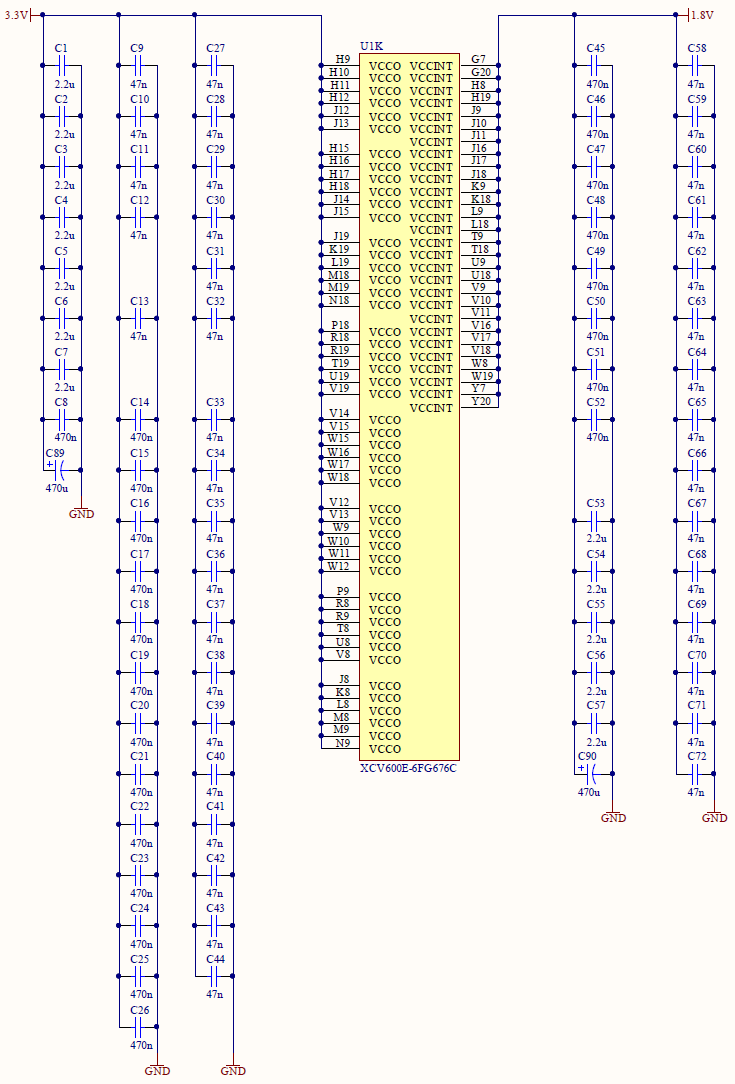
Decoupling an FPGA is always fun. Just look underneath a busy FPGA on a system board to see what I mean. Ideal decoupling depends entirely on the switching needs of your design which of course isn’t possible to know up front on a development board. Xilinx do publish guidance in XAPP623 based on ascending capacitor decades and a table of percentage weights given to each decade that allow you to figure out how many of each you should select. I used this guide as a reference and selected proportions of 47n, 470n and 2.2µ ceramic capacitors. Bulk capacitance is supplied by a pair of 470µ electrolytics, one each on the 1.8V and 3.3V supplies.
GPIO bank
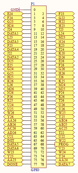
I’ve exposed 78 GPIOs here which ought to be enough to keep me happy for the forseeable future. You can’t see it in the diagram but this row of GPIOs is arranged as a 39×3 block with the column running down the middle connected to GND. This arrangement allows me to connect a 2-row IDC ribbon cable directly to the GPIO block and have every other pin being GND. This is a common arrangement used to maintain signal integrity in a single-ended parallel cable. See the layout of the wires on a JTAG cable for a good example of this in practice.
Differential pairs
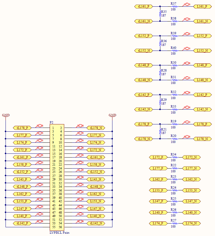
I’ve chosen to expose as many of the FPGA’s differential pairs as I can route out and these can of course be used for normal single-ended signals as well. Unfortunately these old FPGAs don’t support on-chip dynamic impedence matching so you should terminate the differential pairs on the PCB. Xilinx recommends serial termination for receivers and series-parallel termination for transmitters. I’ve included roughly equal numbers of pairs terminated as transmitters and receivers on this board.
Static RAM
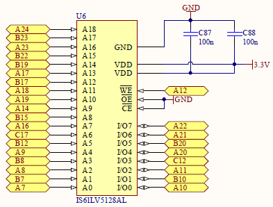
I said in the introduction that I was going with a theme of external memory interfaces on this board and I’ve got started here with a 512kb chunk of SRAM, the IS61LV5128AL 8-bit 10ns part from ISSI. I know this part well from my previous FPGA graphics accelerator project so driving it here won’t be a problem.
SDRAM
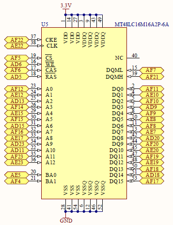
Static RAM is simple to drive and has very fast random access characteristics but it’s too expensive to produce in large sizes and that’s where DRAM comes in. The part that I’ve selected is the 256Mb 16-bit Micron MT48LC16M16A2P-6A. As a single data rate (SDR) 166MHz device it should not be difficult to drive and won’t require the difficult PCB routing that you get with the recent DDR chips.
Flash
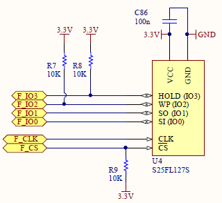
Here’s another one that I used before in the FPGA graphics accelerator project. It’s a 128Mb S25FL127S SPI serial part from Spansion. I know it well and I’ve driven it in the very fast 4-bit mode so I know what to expect from this one.
LEDs and switches
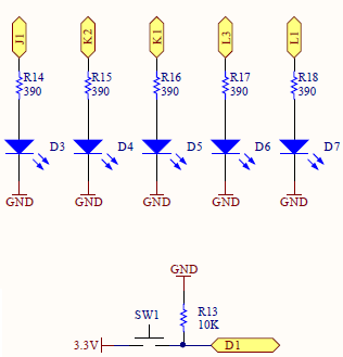
It wouldn’t be the same without a light or two to flash. Seriously though, FPGAs are not easy to debug and it can be invaluable to have the ability to just switch on a LED. There’s five of them on this board as well as a PCB button for user input.
Programming
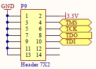
Xilinx FPGAs offer a multitude of programming options. In my previous projects I’ve used the slave serial mode that allows an external intelligent device, in my case an MCU, to load up the FPGA configuration at boot time using a SPI-like protocol to the FPGA. This makes sense for a complete embedded design but doesn’t work for a development board where the JTAG connector is far more useful. I’ll provided one of those 14-pin JTAG socketed headers that will accept a standard IDC cable from a Xilinx platform USB programmer.
Bill of materials
I’m not expecting anyone to actually want to build this as a complete development board but just in case, here’s the full bill of materials.
| Identifiers | Value | Quantity | Description | Footprint |
|---|---|---|---|---|
| C1, C2, C3, C4, C5, C6, C7, C53, C54, C55, C56, C57 | 2.2µ | 12 | Ceramic capacitor | 0402 |
| C8, C14, C15, C16, C17, C18, C19, C20, C21, C22, C23, C24, C25, C26, C45, C46, C47, C48, C49, C50, C51, C52 | 470n | 22 | Ceramic capacitor | 0402 |
| C9, C10, C11, C12, C13, C27, C28, C29, C30, C31, C32, C33, C34, C35, C36, C37, C38, C39, C40, C41, C42, C43, C44, C58, C59, C60, C61, C62, C63, C64, C65, C66, C67, C68, C69, C70, C71, C72 | 47n | 38 | Ceramic capacitor | 0402 |
| C73 | 15p 5% | 1 | Ceramic capacitor | 0603 |
| C74, C81, C82, C83, C84 | 22µ | 5 | Ceramic capacitor | 0805 |
| C75 | 470n | 1 | Ceramic capacitor | 0603 |
| C76, C78 | 10µ | 2 | Ceramic capacitor | 0805 |
| C77 | 8200p | 1 | Ceramic capacitor | 0603 |
| C79, C80, C85, C86, C87, C88 | 100n | 6 | Ceramic capacitor | 0603 |
| C89, C90 | 470µ | 2 | Electrolytic capacitor | Radial 4x8x12mm |
| D1 | Schottky | 1 | ST Micro STPS3L40S | DO-214AB |
| D2 | red LED | 1 | Power LED | 0603 |
| D3, D4, D5, D6, D7 | red LED | 5 | Indicator LEDs | 2012 |
| L1, L2 | 3.3µ | 2 | LQH44PN3R3MP0L | 4x4mm |
| P1 | GPIO Header 39x3 | 1 | 39x3 pin header | 2.54mm |
| P2 | GPIO Header 28x2 | 1 | 28x2 pin header | 2.54mm |
| P3 | USB mini B | 1 | USB power entry | SMD |
| P4 | Header 1x4 | 1 | 1.8V power header | 2.54mm |
| P5 | Header 1x2 | 1 | GCK2 input | 2.54mm |
| P6 | Header 1x2 | 1 | 50MHz oscillator enable | 2.54mm |
| P7 | Header 2x6 | 1 | CLK/MODE header | 2.54mm |
| P8 | Header 1x5 | 1 | PROG header | 2.54mm |
| P9 | Header 2x7 | 1 | JTAG IDC boxed header | 2.54mm |
| P10 | Header 2x2 | 1 | 3.3V power header | 2.54mm |
| P11 | Header 1x4 | 1 | 5V power header | 2.54mm |
| R1 | 27k 1% | 1 | SMD resistor | 0603 |
| R2 | 100k | 1 | 0603 | |
| R3 | 20k 1% | 1 | 0603 | |
| R4 | 45.3k | 1 | 0603 | |
| R5, R7, R8, R9, R10, R11, R12, R13 | 10k | 8 | 0603 | |
| R6, R14, R15, R16, R17, R18 | 390 | 6 | 0805 | |
| R19, R20, R22, R23, R24, R25, R26, R27, R30, R31, R32, R33, R34, R37, R38, R39, R40, R41, R42, R43 | 100 | 20 | 0402 | |
| R21, R28, R29, R35, R36 | 187 | 5 | 0402 | |
| SW1 | Button | 1 | PCB mount button | through hole |
| U1 | XCV600e FPGA | 1 | Xilinx Virtex-e | FG676 BGA |
| U2 | LMR10515 | 1 | TI switching regulator | SOT23-5 |
| U3 | TPS54339DDA | 1 | TI switching regulator | SO-8 powerpad |
| U4 | S25FL127S | 1 | Spansion 128Mb flash | SO-8 (208mil) |
| U5 | MT48LC16M16A2P-6A | 1 | Micron SDRAM | TSOP2-54 |
| U6 | IS61LV5128AL | 1 | ISSI 512Kb SRAM | TSOP2-44 |
| X1 | ASE-50.000MHZ-LR-T | 1 | Abracon 50MHz oscillator | 3.2x2.5mm |
PCB Design and Layout
I stated earlier that I would be constraining the board size to 10x10cm so that I can qualify for an affordable prototype four layer service. The next decision to make is the layer stackup.
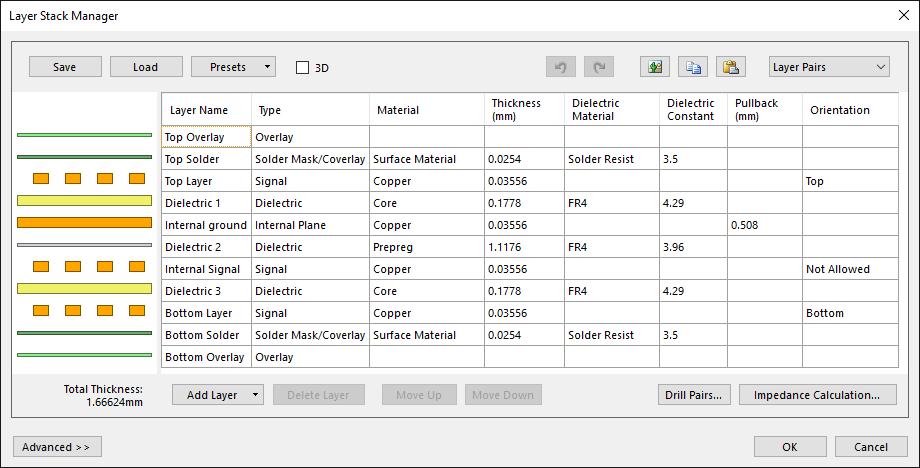
I went for a commonly used arrangement of signal – ground – power/signal – signal. Having a ground plane directly below the top means that I can do impedance controlled routing on the top layer with traces that don’t have to be very wide. All the differential pairs are set to the correct 12.3 mil width for 50Ω impedance control on this board.
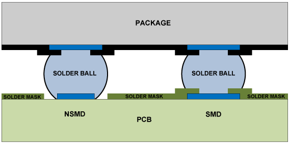
During the early days of BGA design there was some debate over whether pads should be Solder Mask Defined (SMD) or Non-Soldermask Defined (NSMD). As you can see from the diagram SMD pads are defined only by an aperture in the soldermask. NSMD pads are your regular type where the soldermask is pulled back a little to expose a narrow gap where you can see bare board. The preference these days is for NSMD for all footprints except in some extreme exceptions where an ultra-fine pitch might lead to bridging. That’s not the case for me so it’ll be NSMD for the BGA footprint on my board.
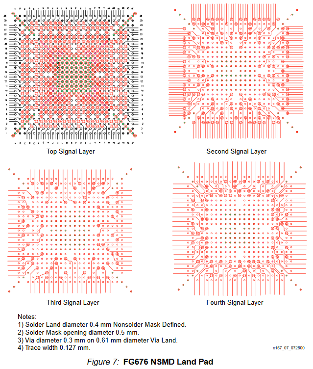
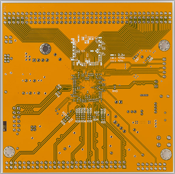
All the major components are on the top layer and hence that’s where the majority of the traces are routed. Let’s have a closer look at the BGA escape routing.
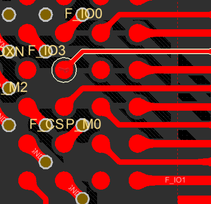
The pads are routed either to a via or to the edge of the footprint with 6 mil traces where they then expand to a wider trace for further routing across the board. The vias are all 0.3mm hole size with an overall diameter of 0.4mm. Teardrops were enabled across the entire design to ensure a stronger bond between pad and trace.

All the differential pairs are length as well as impedance matched. This meant adding these funky looking snake traces to keep the lengths within a few mills of each other. An additional design rule keeps the differential pairs at least 20 mils away from the ground fill on the top layer as well.
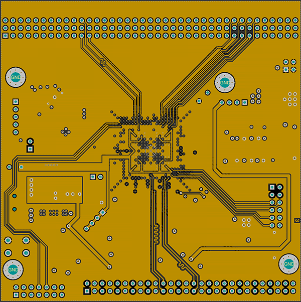
The internal signal layer has a 3.3V flood fill which takes care of many of the power connections. The 1.8V supply is routed using traces. A small number of signal traces are also routed on this layer
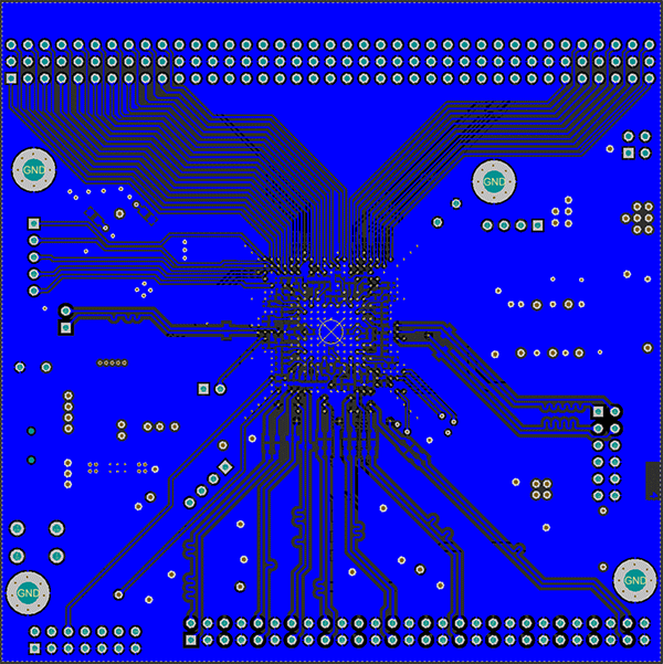
The bottom layer has the remaining traces, mainly those going out to the GPIO header and some others going to the differential pin headers. The traces on the bottom layer are not 50Ω controlled due to the lack of a ground plane directly below them.
The design is now ready to be manufactured so all that remains is to export it as a set of Gerbers and upload it to my choice of the Chinese prototype houses. I’ve been using PCBWay lately for all four layer designs because the results have been consistently good and with this board I don’t really want to be venturing into the unknown by taking a punt on a slightly cheaper manufacturer.
The board thickness will be the full 1.6mm because I don’t want any accidental flexing of this board that could crack the BGA joints. Navigating their site was easy enough and the final price with slow shipping was around 65 American bucks for ten copies.
The blank boards have arrived
It’s normally about three or four weeks from the date of the design upload to it arriving back in the UK and this was no exception. Patience is a virtue when using the HK Post shipping service. Here’s how they look, top and bottom. I’ve grown to like the mustard-yellow soldermask with white silkscreen and will probably use it more in the future.
The choice of finish for your pads can either be HASL or the more expensive ENIG (that’s the gold coloured one). ENIG has the advantage of producing a totally flat finish but costs a fair bit more. I did some research and ENIG is favoured for BGA footprints of less than 0.8mm pitch. Above that HASL is fine. Mine is a 1mm pitch BGA so I went with HASL to save on the costs.
At first glance the PCBs appear to be as well manufactured as I’ve come to expect from PCBWay’s four layer service. Drill registration is spot on and all the narrow soldermask slivers are intact. However, inspection under the microscope did show that a few of the boards had minor manufacturing defects in the BGA footprint area.
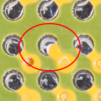
As you can see from this close up the soldermask has spilled over to partly obscure one of the pads. This is not good, but I did expect that I wouldn’t get a 100% result from a prototype service on a BGA footprint this large and that was the main reason for me ordering 10 boards and not the cheaper 5. Most of the boards were defect-free though, and now I could move on to the reflow process.
Testing the reflow procedure
My plan is to apply generous quantities of my Amtech flux to the board, seat the FPGA on the footprint and then to run a standard SnPb reflow profile. In my opinion there’s plenty of solder in the balls themselves and no need for me to go to the considerable extra expense of a stencil and solder paste just to put even more solder onto the pads. Flux will be key here. Good wetting of the pads will ensure a reliable joint. Too little and I’ll get dry joints. Too much and the whole package can float off across the board as the flux boils underneath the part which can be amusing when it happens to someone else.
Looking at simple economics I have boards that cost about a fiver, FPGAs that cost about 2 quid and a bunch of peripheral parts that together cost about 20 quid. It makes sense to reflow an FPGA on its own as a test. If the process works then I go ahead and do a full board with all parts on board.
Well, it worked. There were no dramas during the process and I think it’s fully reflowed but without some kind of X-ray analysis I’ll never know for sure.
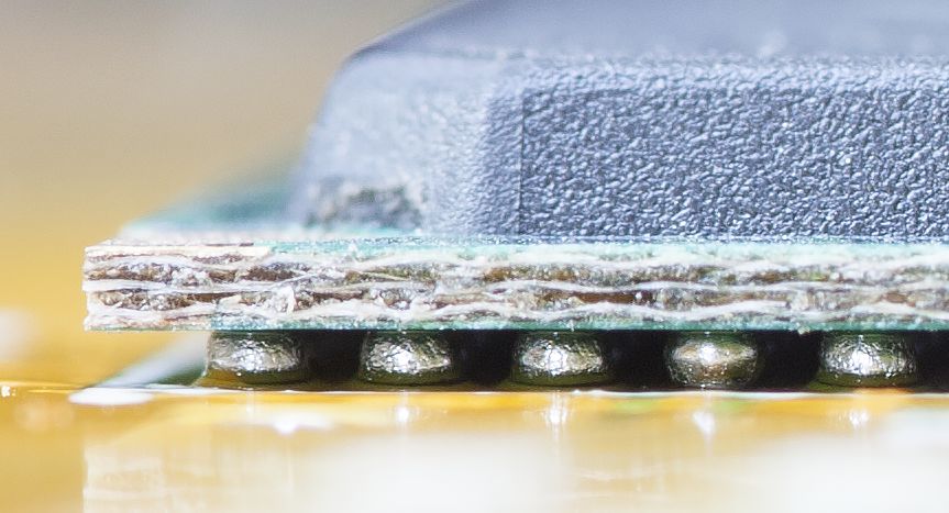
The best I can do is this high resolution photograph using a macro lens and a set of extension tubes. I can see that the balls at all four corners of the package have gone flat at the bottom where they meet the pad. That should mean that all the central balls have done the same but I can never be completely sure. I decided to go ahead and do a full board.
Reflow and testing
I reflowed all the major parts on the top of the board at the same time, from the FPGA and the memory ICs right down to the 0402 termination resistors. It all went fine. Then I needed to add sufficient parts to the board to be able to validate what I’d done with a simple FPGA design. That’s when I realised that I’d made my job a lot harder than it need be.
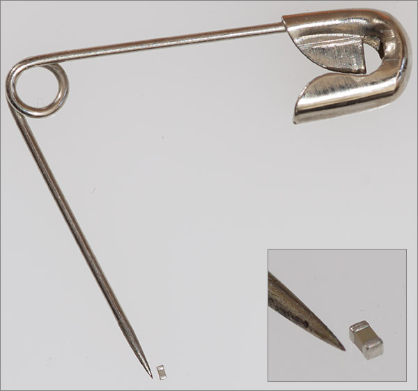
An 0402 capacitor next to a safety pin
I needed to mount all the 0402 decoupling capacitors on the bottom of the board and I did so using a hot air gun and a pair of tweezers and boy was there much swearing involved. I know there are people out there that claim to be able to hand solder 0402s in the dark using a plumbers iron and a pair of pliers for tweezers. Well that’s not me. It must be an age thing because I just can’t focus properly on the damn things any more. It took a while, and I got most of them down on the board and at least the same number somewhere on my carpet or in my hair.
With the benefit of hindsight I should have reflowed the bottom side in the reflow oven, kapton taped them in place and then done the top side. Much pain would have been avoided. Afterwards I rushed off and bought one of these on ebay.
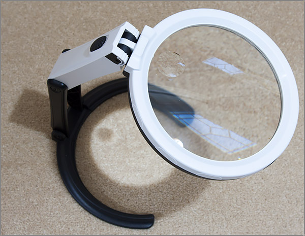
Revelation! The large working distance, big lens and LED ring light work really well. Now I can see those little 0402s just like they were 0603s. I highly recommend this cheap piece of kit.
Minimal assembly prior to testing
I’ve added just enough components to be able to do a test, so it’s over to the Xilinx ISE software for some VHDL fun.
Xilinx ISE 10.1
The latest version of ISE to support the Virtex-E is 10.1 and that’s only supposed to work on Windows XP. There are forum posts from people who’ve managed to get it working on more recent Windows editions but since it only takes half an hour to spin up an XP virtual machine using the free VMWare Player then that’s what I did.
The final link is the JTAG programmer used to upload the design bitstream to the FPGA. I have a Platform USB programmer that I got on ebay from, yes you guessed it, China for about 20 quid. It features the Xilinx logo on the box but I’d be surprised to find that it’s genuine because I don’t think Xilinx have ever charged as little as 20 quid for anything frankly.
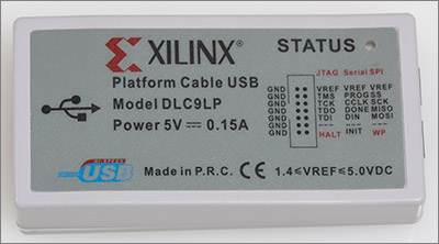
Genuine Xilinx? Hmmm.
This’ll be the first time that I’ve used it so we’ll see if it works. Now all I need is an FPGA design to exercise the board. There’s a row of five LEDs on this board so I decided to go for a PWM flashing thing. I’d bring the LEDs up to 100% brightness and then fade them down to zero with a little delay between each one so it looks a bit like a progression along the line of LEDs.
To do the fading effect I’ll need a process that can output a PWM signal on one of the GPIO lines. Here’s what it looks like.
library ieee;

use ieee.std_logic_1164.all;
use ieee.numeric_std.all;


-- Very simple PWM implementation. The 50MHz clock on the
-- virtex-e development board will yield a frequency of 500kHz
-- Frequency = clk_in / 100
-- Duty cycle = 0..100

entity pwm is
  port(
    clk_in     : in  std_logic;
    duty_cycle : in  std_logic_vector(6 downto 0);
    pwm_signal : out std_logic
  );
end pwm;

architecture behavioral of pwm is

  -- a 7 bit counter is wide enough to hold 0..100

  signal counter_i : std_logic_vector(6 downto 0) := (others => '0');
  signal pwm_signal_i : std_logic := '0';

begin

  -- wire up the output

  pwm_signal <= pwm_signal_i;

  process(clk_in)
  begin

    if rising_edge(clk_in) then

      -- if the counter has passed the current dury cycle percentage then set the signal low
      -- otherwise it remains high

      if counter_i >= duty_cycle  then
        pwm_signal_i <= '0';
      else
        pwm_signal_i <= '1';
      end if;

      -- if the counter is at 99 then reset it back to 0 for the next PWM clock cycle
      -- otherwise just increment it.

      if counter_i >= std_logic_vector(to_unsigned(99,counter_i'length)) then
        counter_i <= (others => '0');
      else
        counter_i <= std_logic_vector(unsigned(counter_i)+1);
      end if;

    end if;

  end process;

end behavioral;
Now I need a process that will use the PWM component to fade a LED from 100% duty cycle down to zero. Here it is.
library ieee;

use ieee.std_logic_1164.all;
use ieee.numeric_std.all;

-- The fader component manages resetting a LED to 100% duty cycle and then fading
-- it down to zero using the PWM component. The fade time is about 1.6s

entity fader is
  port (
    clk_in  : in  std_logic;
    restart : in  std_logic;
    led_out : out std_logic
--add a few more signals to the simulator
--pragma synthesis_off
    ;
    duty_cycle_sim : out std_logic_vector(6 downto 0);
    fader_clk_sim : out std_logic
--pragma synthesis_on
  );
end fader;

architecture behavioral of fader is

  component pwm port(
    clk_in     : in  std_logic;
    duty_cycle : in  std_logic_vector(6 downto 0);
    pwm_signal : out std_logic
  );
  end component;

  -- 7 bit duty cycle and 18 bit counter

  signal duty_cycle_i : std_logic_vector(6 downto 0) := (others => '0');
  signal clk_gen_counter_i : std_logic_vector(17 downto 0) := (others => '0');
  signal fader_clk_i : std_logic := '0';

begin

--pragma synthesis_off
  duty_cycle_sim <= duty_cycle_i;
  fader_clk_sim <= fader_clk_i;
--pragma synthesis_on

  -- instantiate a PWM component to manage the fade to zero

  inst_pwm : pwm port map(
    clk_in     => clk_in,
    duty_cycle => duty_cycle_i,
    pwm_signal => led_out
  );

  -- generate a slow clock from the 50MHz input clock using a prescaler

  slow_clk_gen: process(clk_in)
  begin

    if rising_edge(clk_in) then

      clk_gen_counter_i <= std_logic_vector(unsigned(clk_gen_counter_i) + 1);

      if clk_gen_counter_i > std_logic_vector(to_unsigned(150000,clk_gen_counter_i'length)) then
        fader_clk_i <= not fader_clk_i;
        clk_gen_counter_i <= (others => '0');
      end if;

    end if;

  end process;


  -- Manage the fade process. If restart is asserted then the duty cycle
  -- is reset back to 100. Otherwise we slowly fade down to zero then stop.

  fade_process: process(fader_clk_i)
  begin

    if rising_edge(fader_clk_i) then

      if restart = '1' then
        duty_cycle_i <= std_logic_vector(to_unsigned(100,duty_cycle_i'length));
      else

        if duty_cycle_i /= "0000000" then
          duty_cycle_i <= std_logic_vector(unsigned(duty_cycle_i) - 1);
        end if;

      end if;
    end if;

  end process;

end behavioral;
Now I have the ability to fade a LED from 100% down to zero I need to instantiate five copies of it and manage the timing so that each of the five LEDs starts slightly after the previous one. This is the main, top-level VHDL module and it looks like this:
library ieee;

use ieee.std_logic_1164.all;
use ieee.numeric_std.all;

-- Top level component. clk_in is bound to the onboard 50MHz oscillator that is routed
-- to one of the GCLK inputs. The 5 LED outputs are wired up to the 5 red LEDs on
-- the development board

entity main is
  port (
    clk_in    : in  std_logic;
    led_1_out : out  std_logic;
    led_2_out : out  std_logic;
    led_3_out : out  std_logic;
    led_4_out : out  std_logic;
    led_5_out : out  std_logic
  );
end main;

architecture behavioral of main is

  -- definition of the fader component

  component fader port(
    clk_in  : in  std_logic;
    restart : in  std_logic;
    led_out : out std_logic
  );
  end component;

  -- we need a 23 bit counter to generate the slow clock

  signal clk_gen_counter_i : std_logic_vector(22 downto 0) := (others => '0');
  signal led_restart_i : std_logic_vector(4 downto 0) := (others => '0');
  signal led_clk_i : std_logic := '0';

begin

  -- instantiate 5 copies of the fader component, one for each of
  -- the onboard LEDs. Each of the restart signals is bound to a
  -- bit in the led_restart array.

  inst_fader_1 : fader port map(
    clk_in  => clk_in,
    restart => led_restart_i(4),
    led_out => led_1_out
  );
  inst_fader_2 : fader port map(
    clk_in  => clk_in,
    restart => led_restart_i(3),
    led_out => led_2_out
  );
  inst_fader_3 : fader port map(
    clk_in  => clk_in,
    restart => led_restart_i(2),
    led_out => led_3_out
  );
  inst_fader_4 : fader port map(
    clk_in  => clk_in,
    restart => led_restart_i(1),
    led_out => led_4_out
  );
  inst_fader_5 : fader port map(
    clk_in  => clk_in,
    restart => led_restart_i(0),
    led_out => led_5_out
  );

  -- generate a slow clock from the onboard 50MHz oscillator using a prescaler

  process(clk_in,led_clk_i)
  begin

    if rising_edge(clk_in) then

      clk_gen_counter_i <= std_logic_vector(unsigned(clk_gen_counter_i) + 1);

      if clk_gen_counter_i > std_logic_vector(to_unsigned(6250000,clk_gen_counter_i'length)) then
        led_clk_i <= not led_clk_i;
        clk_gen_counter_i <= (others => '0');
      end if;

    end if;

  end process;


  -- use the slow clock to advance through the LEDs one at time. A shift register
  -- moves a single 'restart' bit from left to right causing the fader component
  -- that's listening on that bit to restart its fade

  process(led_clk_i)
  begin

    if rising_edge(led_clk_i) then

      if led_restart_i = "00000" or led_restart_i = "00001" then
        led_restart_i <= "10000";
      else

        -- this is a right shift
        led_restart_i <= '0' & led_restart_i(4 downto 1);

      end if;

    end if;

  end process;

end behavioral;
That's about all really. The only other important file is the .ucf file that defines which pads the nets are connected to as well as any timing constraints that I might have. Here's what it looks like.
NET "clk_in" LOC = E13;
NET "led_1_out" LOC = J1;
NET "led_2_out" LOC = K2;
NET "led_3_out" LOC = K1;
NET "led_4_out" LOC = L3;
NET "led_5_out" LOC = L1;

NET "clk_in" TNM_NET = "clk_in";
TIMESPEC TS_clk_in = PERIOD "clk_in" 20ns HIGH 50 %;
Five LEDs and the 50MHz oscillator input on a GCLK net. That's all there is. Just to be sure I added a timing constraint that tells the compiler the frequency of my oscillator so that it can make sure that my timing constraints are met. Not that there's much danger of me tripping over that one with this simple design.
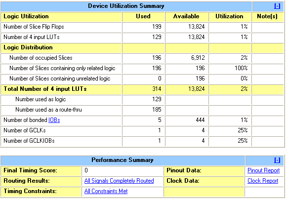
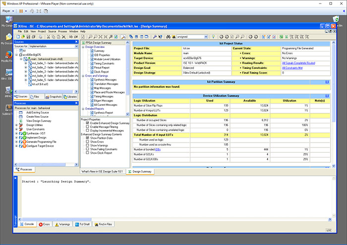
ISE compiled the design with no fuss and I had a bistream waiting for me to upload into the FPGA. I connected power to the board through the USB connector and then hooked up the platform USB cable. After redirecting the USB device to the XP virtual machine a green LED appeared on the programmer's front panel. That must a good thing, green is always good. Xilinx Impact is the program used to talk JTAG to the FPGA so I fired it up and created a new 'project' based around the .bit file generated by ISE.
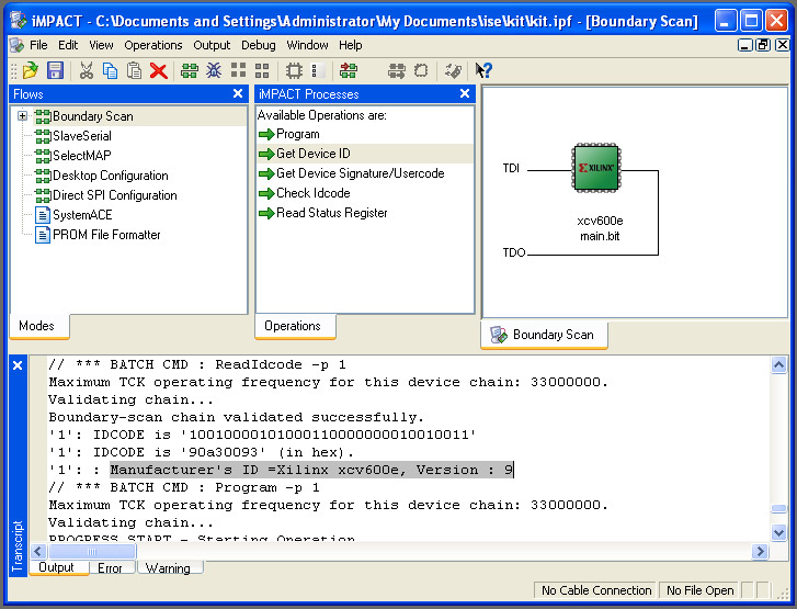
It worked! I was massively relieved and pleased to see that the FPGA was recognised by Impact as the correct device type which means that it was definitely alive. Well, at least the JTAG pins were alive and well. Without further ado I hit the Program button to see what would happen.
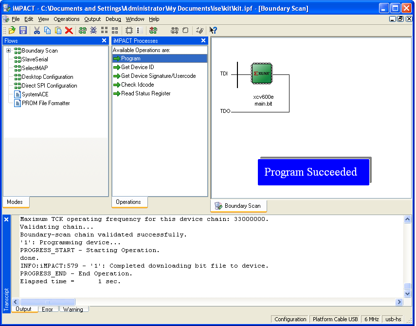
Wahey! It's working! Yes, of course it took a few iterations around the develop/compile/test cycle to get the timings right but there it was, working perfectly.
Never has blinkenled meant so much
Now I know that the FPGA core and IOs are fine. The JTAG interface, the oscillator and at least the I/Os that I've tested are all good. I'll just stare at these LEDs for a few minutes if you don't mind and then I'll go put the rest of the board together.
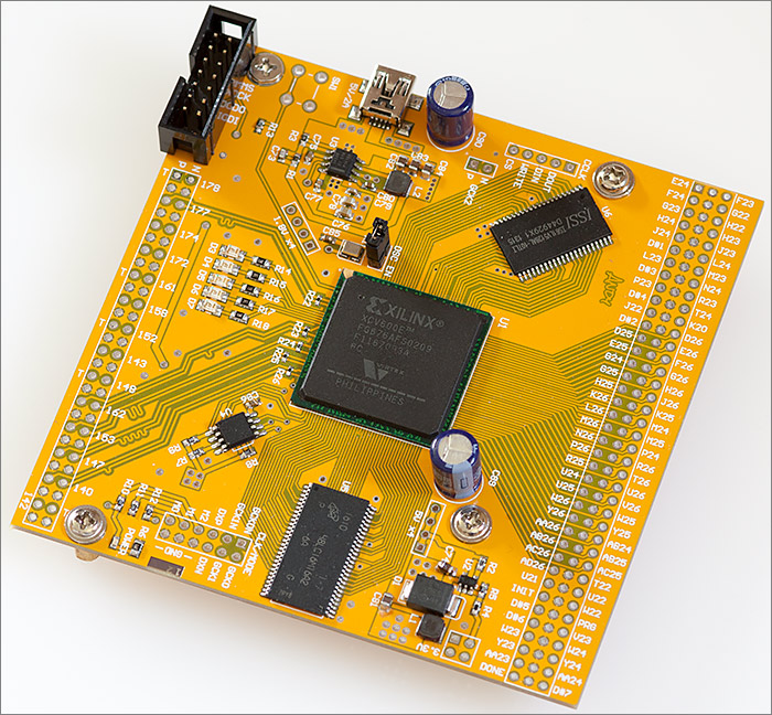
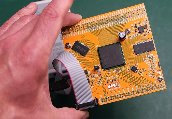
A fully assembled board
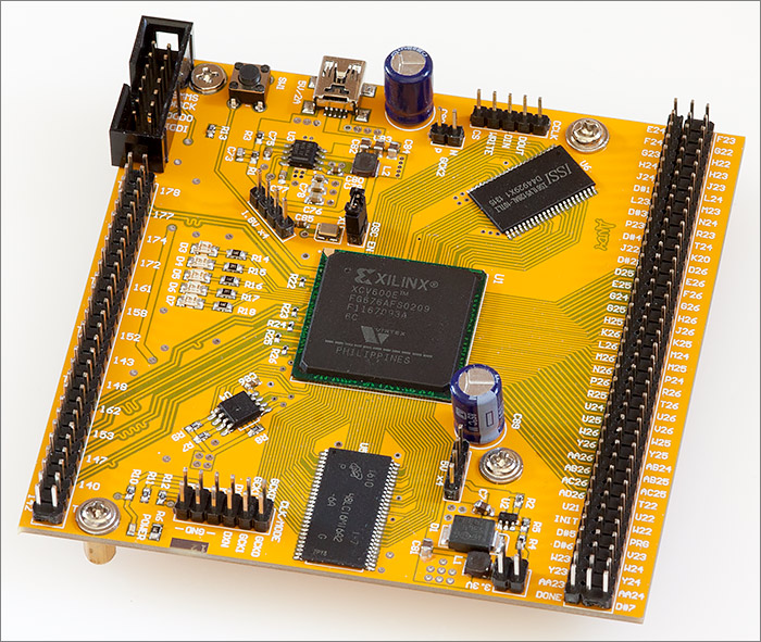
So there it is, all fully assembled and looking really nice. This has been an interesting project for me and I've learned a lot of new things along the way. I know now that BGAs can be reflowed by hobbyists as long as we can have the boards manufactured at reasonable cost. Best of all is that I've got a nice Virtex FPGA development board that I can play around with.
Video and final words
I've put together a video of my experience creating this design and you can watch it here on YouTube. Alternatively head off over to the main youtube site and wach it in full HD.
I hope you've enjoyed reading this write-up and perhaps watching the video as much as I enjoyed creating them. Please feel free to leave your comments in the section below or maybe you'd like to chat about this project over in the forum.
Until next time, take care and happy hacking!