Tags
Related Posts
Share This


Project Difficulty
- All components are commonly available.
- The smallest IC pin pitch is 0.65mm
- The smallest discrete component is 0603.
- All components are on the top-side of the board
Recent Posts
A development board for the STM32F042 TSSOP package
It’s been a while since I posted a new article, a delay at least partly due to me herniating a disc in my neck which left me completely unable to look downwards for any length of time and as you’ll know all too well you can’t work on circuit boards without peering down at them. Look after your neck and back folks, and I mean that seriously.
Well I’m back now and I’ve got a lot of ideas for articles spinning around in my head that will hopefully come to fruition over the next few months. First off the block is this one in which I’m going to present a simple development board for the STM32F042 in the easy(ish) to work with TSSOP20 package.
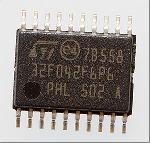
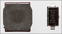
STM32F042 TSSOP20 0.65mm pitch package
This project came about because I’m using the STM32F042F6P6 (32Kb flash, 6Kb SRAM) in another project where I’m creating a USB device and the first thing I did is try to obtain a development board for it. I was hopeful that ST would have created one of their ‘discovery’ boards but no, there was only a ‘nucleo’ board available and that had one of the QFP packages on it.
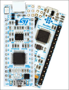
The F042 nucleo board
The nucleo board would have probably been sufficient for my needs but I do prefer to work on the actual device that’s going to be used in the real project and I had a few ideas for features that I’d include that I wish would be included in other development boards but never seem to be.
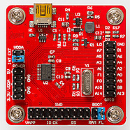
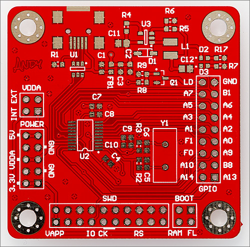
Development board features
Schematic
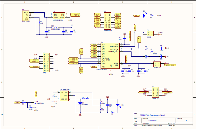
The schematic is rather modular so let’s take a look at each section in detail.
The power supply
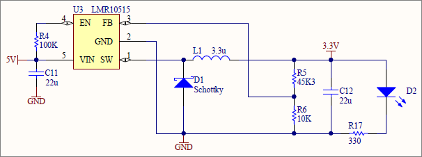
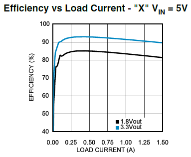
The 3.3V voltage for the board is supplied by a Texas Instruments LMR10515 adjustable switching buck (step-down) regulator. I’ve used this regulator a few times before and have found it to be a solid and reliable device that doesn’t require many external components and only costs about 50 pence from Farnell.
This regulator is capable of supplying up to 1.5A with an efficiency level of over 90% throughout most of its range. The input will be the 5V VBUS line from the USB plug after I’ve sanitised it to remove the gremlins that lurk therein.
It’s this efficiency level that allows switching regulators to deliver their peak current rating without burning up in a puff of smoke. The output inductor and schottky diode must both be chosen to match the desired peak current from the regulator. For the inductor I’ve chosen the Murata LQH44PN3R3MP0L (2.1A maximum current) and for the schottky I’m using an ST Micro STPS0520Z (0.5A maximum current).
In practice this means that my development board is limited to 500mA but you can use any schottky that will fit the SOD-123 footprint if you need a higher current supply up to the 1.5A maximum that the regulator can deliver.
The MCU
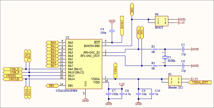
The MCU power and reset scheme is wired up according to ST’s recommendations. VDD gets a pair of 100nF and 4.7µF capacitors and VDDA gets a 10nF and 1µF pair. P3, a 4 pin header, receives a jumper across pins 1 and 2 to connect VDDA to the onboard 3.3V supply or the jumper can be removed to allow an external VDDA to be connected to pin 3.
C4 decouples the active-low reset pin to prevent any spurious resets from ruining your day. There’s no need for a pull-up to VDD because ST supply one internally.
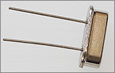
The crystal is connected to the MCU via a pair of 0R ‘resistor’ bridges that can be removed if you’ve fitted a crystal but want to use the PF0 and PF1 pins as GPIO without fear of interference from the crystal itself.
If you’re considering USB device development and you’ve done this before then you may think that you’re going to need the external crystal to generate the accurate 48MHz clock required by USB to stay in sync with the host, but this is not the case. ST supply an internal ‘HSI48’ 48MHz clock specifically for use with the USB peripheral and with a bit of software configuration you can not only clock the MCU core from it but you can also constantly trim its accuracy from the USB Start of Frame (SOF) packets sent by the host to the device every 1ms. I’ll show you how to set up this crystal-less configuration later on.
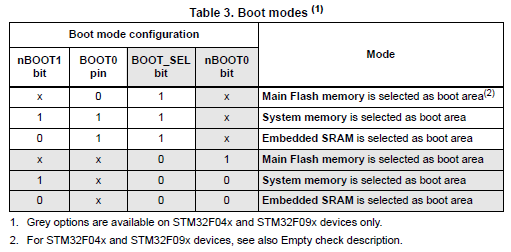
Upon startup the MCU can boot from flash, SRAM or system memory (that’s where the boot loader is). The most common option is to boot from flash directly into your code and you select that by holding BOOT0 low during the exit from reset and standy modes.
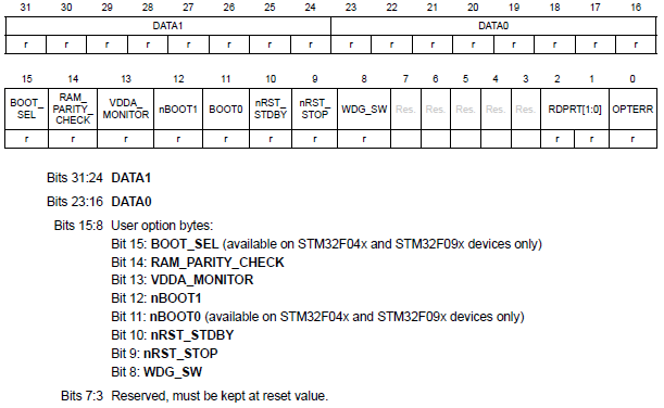
But wait, doesn’t this waste the PB8 GPIO pin? No it doesn’t. If you always want to boot from flash then you can program the BOOT_SEL and nBOOT0 bits of the FLASH_OBR register to 0 and 1 respectively and then the MCU will ignore BOOT0 and you can use it as a GPIO pin.
Programming and debugging
ST include an embedded ST-Link/v2 chip on their discovery boards implemented within an STM32F1 series MCU that allows you to program and debug over the same USB line that you use to supply power.
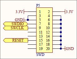
That’s neat, and it means that you don’t have to buy a programmer for your board. It is, however, proprietary which means I can’t include it on this board. Instead, I include the standard 20-pin ST-Link/v2 header that you can attach a programming cable to.
I’ve already written an article about how to set up and use the ST-Link/v2 programmer using only free software.
The USB interface
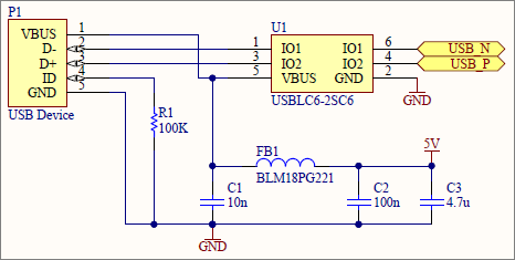
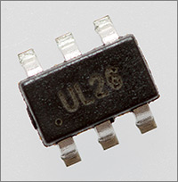
I’ve opted to include an ST Micro USBLC6-2SC6 ESD protection device between the USB lines and the MCU. Without this the MCU would be vulnerable to ESD events on the line caused by handling of the plug or cable and could easily be damaged or destroyed.
Chances are you don’t even have the ID signal line in your cable (it’s for OTG cables only) but in common with ST’s configuration on their discovery boards I’m grounding it through a 100kΩ resistor.
C1, C2, C3 and FB1 form a filtering network to remove noise from the VBUS line before it becomes an input to the switching regulator. If you’ve never seen how much noise you can get on VBUS then I recommend that you take a look at this article that I wrote.
If you’re powering this board from a computer’s USB port then be mindful of the maximum amount of power that you can draw. This wikipedia article explains it well. Of course if you’re powering this board from a USB wall charger then the limit is set by that charger.
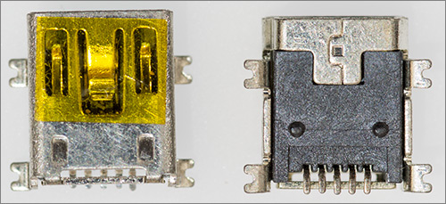
The USB socket itself is a mini-B size and has a very common standard footprint. Search ebay for these mini-B PCB sockets and you’ll see that they all have this footprint.
Power output
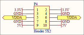
P4 is a pin header that can be used to access the power supplies on the board along with a generous helping of ground pins. You can’t have too many ground pins on a development board and I find it really frustrating when you receive a board to find it’s only got one or two ground pins. I’ve included four here and another one on the GPIO header.
NPN transistor
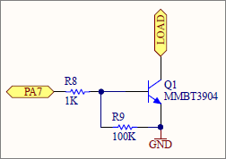
The base of the MMBT3904 transistor is connected via a 1kΩ resistor to PA7 so you can control it as a switch from the MCU. The maximum collector current for the MMBT3904 is 200mA. If you need more than that then you should substitute this part for another one in the SOT23-3 package that has a higher rating.
R9, a 100kΩ resistor, pulls the base down to ground so you don’t get spurious switching events during any periods when the gate is floating. The idea is that you connect your load to be driven to the LOAD pin.
GPIO
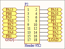
All the GPIO pins exposed by the TSSOP20 package are included here as well as the LOAD pin for the NPN transistor and an additional ground pin.
Bill of materials
Here’s the full bill-of-materials for this board, along with Farnell product code numbers to help you put together an order basket.
| Identifiers | Value | Quantity | Description | Footprint | Farnell code |
|---|---|---|---|---|---|
| C1, C9 | 10n | 2 | Ceramic capacitors | 0603 | 1709947 |
| C2, C4, C7 | 100n | 3 | Ceramic capacitors | 0603 | 1759122 |
| C5, C6 | 22p | 2 | Ceramic capacitors | 0603 | 2309012 |
| C3, C8 | 4.7µ | 2 | Ceramic capacitors | 0603 | 2320811 |
| C10 | 1µ | 1 | Ceramic capacitors | 0603 | 1759399 |
| C11, C12 | 22µ | 2 | Ceramic capacitors | 0805 | 2309030 |
| D1 | STPS0520Z | 1 | Schottky diode[1] | SOD123 | 1467545 |
| D2, D3 | green , red | 2 | LEDs | 0603 | [2] |
| FB1 | BLM18PG221SN1D | 1 | Ferrite bead[1] | 0603 | 1515740 |
| L1 | LQH44PN3R3MP0L | 1 | Inductor[1] | 4x4mm | 1782797 |
| P1 | USB Mini B | 1 | USB connector | custom | [3] |
| P2 | 1 | Header, 9-Pin, Dual row | 2.54mm | [4] | |
| P3 | 1 | Header, 2-Pin, Dual row | 2.54mm | [4] | |
| P4 | 1 | Header, 5-Pin, Dual row | 2.54mm | [4] | |
| P5 | 1 | Header, 10-Pin, Dual row | 2.54mm | [4] | |
| P6 | 1 | Header, 2-Pin, Dual row | 2.54mm | [4] | |
| Q1 | MMBT3904 | 1 | NPN transistor | SOT23-3 | 1773602 |
| R1, R4, R9 | 100k | 3 | Chip SMD resistor | 0603 | 2447226 |
| R2, R3 | 0 | 2 | Chip SMD resistor | 0603 | 2309106 |
| R5 | 45.3k | 1 | Chip SMD resistor | 0603 | 2059468 |
| R6 | 10k | 1 | Chip SMD resistor | 0603 | 9238603 |
| R7, R17 | 330 | 2 | Chip SMD resistor | 0603 | 2331995 |
| R8 | 1k | 1 | Chip SMD resistor | 0603 | 2447272 |
| U1 | USBLC6-2SC6 | 1 | USB ESD protection | SOT23-6 | 1269406 |
| U2 | STM32F042F6P6 | 1 | MCU | TSSOP-20 | 2469549 |
| U3 | LMR10515 | 1 | Switching regulator | SOT23-5 | 2064682 |
| Y1 | FOXSLF/080-20 | 1 | 8MHz crystal | HC49 | 2063945 |
[1] These components must be rated in excess of the current that you plan to draw. My recommendations support a maximum of 500mA.
[2] 0603 SMD resistors are so cheap on ebay that I recommend you buy some there. I used green for the power LED and amber for the GPIO LED.
[3] The USB mini-B PCB connector is a common footprint that’s very cheaply available on ebay. See the high-resolution photograph in this article and compare to ebay auction photographs.
[4] Dual-row 2.54mm pin headers are very cheap on ebay.
Building the board
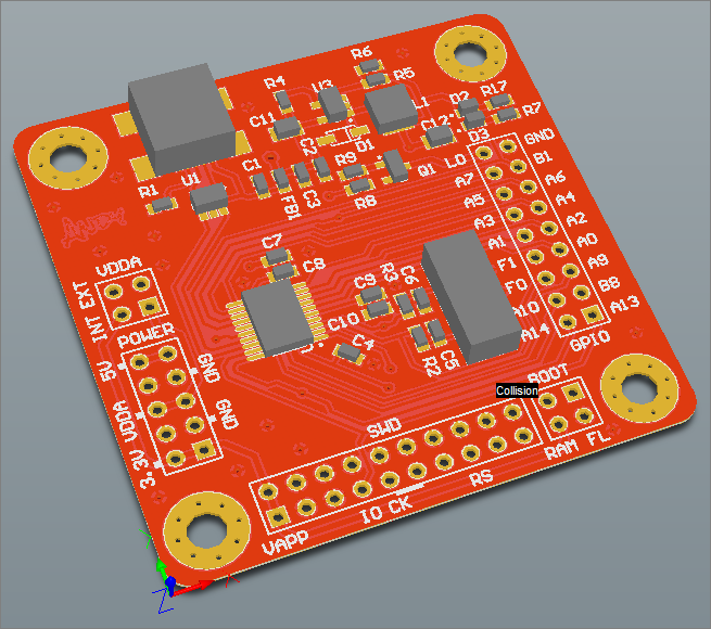
The board was laid out to fit within a 50mm square so that it could be manufactured by one of the discount Chinese prototyping houses such as Seeed, ITead, PCBWay and Elecrow. For this size of board I choose Elecrow and for US$9.90 plus delivery I can get ten copies in about two or three weeks.
Time passes. Two or three weeks worth of time as it happens…
I made a small mistake on the Gerbers for the USB connector. On the footprint I include a guideline on one of the mech layers to aid positioning of the connector at the board edge and I mistakenly included that mech layer on the Gerber export with the result being a small sliver of exposed copper at the board edge on both sides under the USB connector. It makes no difference to the viability of the board but I find it annoying because I know it shouldn’t be there!
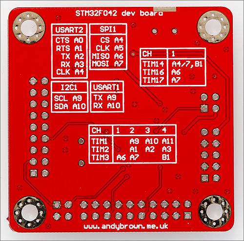
I’ve included M3 sized screw holes that can be used for adding ‘feet’ to the board so it’s lifted above my work surface and if you look at the back you can see that there are some handy quick-reference tables that identify which pins are connected to the commonly used peripherals.
Now it’s time to build it. I don’t have a paste stencil for this board so I opted to build it in several stages. Firstly I tinned all the surface mount pads with solder. Secondly, I reflowed the larger surface mount components such as all the ICs, the inductor and the USB connector using my bluetooth reflow oven. Thirdly I attached all the smaller 0603 and 0805 components using hot air and tweezers and finally the through-hole components were soldered into place using an iron. A quick wash with hot water and fairy liquid followed by drying overnight and she’s ready to test.
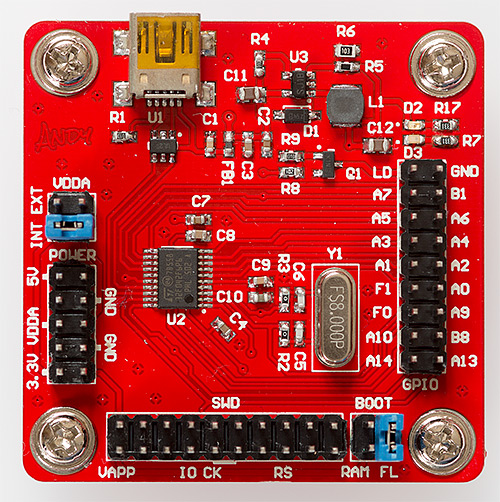
Looking pretty sweet I think. But does it work? Let’s run through some tests to see what it can do.
Testing the functionality
The first test is simply to connect the USB cable from the board to a computer and then test the voltages to make sure the regulator is working. My multimeter read bang on 3.30V from the regulator output and the green power LED, D2, was lit at a nice subtle brightness. Another bugbear of mine is dev boards that include power LEDs configured at retina-burning levels.

Before moving on to a programming test let’s have a look at the residual noise on the board’s 3.3V supply.
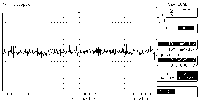
It looks reasonable. Noise levels are within +/- 100mV. Let’s get on with some programming tests. I started up OpenOCD from a Cygwin terminal and got the expected output:
Open On-Chip Debugger 0.9.0 (2015-05-19-12:09)
Licensed under GNU GPL v2
For bug reports, read
        http://openocd.org/doc/doxygen/bugs.html
Info : The selected transport took over low-level target control. The results might differ
       compared to plain JTAG/SWD
adapter speed: 1000 kHz
adapter_nsrst_delay: 100
none separate
srst_only separate srst_nogate srst_open_drain connect_deassert_srst
Info : Unable to match requested speed 1000 kHz, using 950 kHz
Info : Unable to match requested speed 1000 kHz, using 950 kHz
Info : clock speed 950 kHz
Info : STLINK v2 JTAG v17 API v2 SWIM v4 VID 0x0483 PID 0x3748
Info : using stlink api v2
Info : Target voltage: 3.243836
Info : stm32f0x.cpu: hardware has 4 breakpoints, 2 watchpoints
This means that the MCU is responding to the SWD debugging commands and is ready to program. Now to test the onboard features. I’ll use my stm32plus library for all these tests. Even though it does not directly support the F042 series it does support the F051 and with a few adjustments to startup code and linker scripts we should be able to get things going.
Blinky
The first thing we need to do is modify the linker script designed for the F051 to be compatible with the F042. The section at the top needs to be changed to reflect the 32Kb of flash and the 6Kb of SRAM in the F042. These are the changes:
/* End of 6Kb SRAM */
_estack = 0x20001800;

/* Generate a link error if heap and stack don't fit into RAM */

_Min_Heap_Size = 0;      /* required amount of heap  */
_Min_Stack_Size = 0x400; /* required amount of stack */

/* Specify the memory areas */

MEMORY
{
  FLASH (rx)      : ORIGIN = 0x08000000, LENGTH = 32K
  RAM (xrw)       : ORIGIN = 0x20000000, LENGTH = 6K
  MEMORY_B1 (rx)  : ORIGIN = 0x60000000, LENGTH = 0K
}
For now we do not need to modify the code where the core clock is set System.c because it’s already set up to use the PLL fed by the 8MHz HSI. The core clock will be 48MHz.
The onboard LED, D3, is hooked up to PB1. It’s a simple modification to the source code to flash this LED at 1Hz.
void run() {

  // initialise the pin for output

  GpioB<DefaultDigitalOutputFeature<1> > pb;

  // loop forever switching it on and off with a 1 second
  // delay in between each cycle

  for(;;) {

    pb[1].set();
    MillisecondTimer::delay(1000);

    pb[1].reset();
    MillisecondTimer::delay(1000);
  }
}
I fired it up and… success! The amber LED was flashing away at 1Hz. Programming, basic GPIO and the Systick peripheral are all working fine.
The transistor switch
This test is closely related to the basic blinky except this time I connected an external LED and series resistor to the LD (load) pin and change the code to control the blinking to use pin PA7.
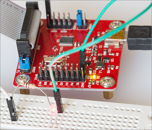
It’s working as expected which validates that the NPN transistor is connected up correctly.
What about the external crystal?
I’m not done with the blinkenled just yet. Before I can move on I need to know if the external 8MHz crystal is working which means configuring it as the MCU clock source. Luckily this is really simple.
If you look inside the System.c startup file you’ll see that ST have provided a simple #define to select the clock source. To configure the HSE as the clock source we merely have to change the code to read like this:
//#define PLL_SOURCE_HSI   // HSI (~8MHz) used to clock the PLL, and the PLL is used as system clock source
#define PLL_SOURCE_HSE           // HSE (8MHz) used to clock the PLL, and the PLL is used as system clock source
//#define PLL_SOURCE_HSE_BYPASS  // HSE bypassed with an external clock (8MHz, coming from ST-Link) used to clock
                                 // the PLL, and the PLL is used as system clock source
Testing a timer
The pin that I’ve attached to the LED, PB1, is also the GPIO output for channel 4 of timer 3. It’s a simple task to set up that timer in PWM mode and then to create a quick demo that pulses the LED as smooth ‘heartbeat’.
void run() {

  Timer3<
    Timer3InternalClockFeature,       // the timer clock source is APB1
    TimerChannel4Feature<>,           // we're going to use channel 4
    Timer3GpioFeature<                // we want to output something to GPIO
      TIMER_REMAP_NONE,               // the GPIO output will not be remapped
      TIM3_CH4_OUT                    // we will output channel 4 to GPIO
    >
  > timer;

  /*
   * Set an up-timer up to tick at 12MHz with an auto-reload value of 1999
   * The timer will count from 0 to 1999 inclusive then reset back to 0.
   */

  timer.setTimeBaseByFrequency(12000000,1999);
  timer.initCompareForPwmOutput();
  timer.enablePeripheral();

  /*
   * It's all running automatically now, use the main CPU to vary the duty cycle up
   * to 100% and back down again
   */

  for(;;) {

    // fade up to 100% in 4ms steps

    for(int8_t i=0;i<=100;i++) {
      timer.setDutyCycle(i);
      MillisecondTimer::delay(4);
    }

    // fade down to 0% in 4ms steps

    for(int8_t i=100;i>=0;i--) {
      timer.setDutyCycle(i);
      MillisecondTimer::delay(4);
    }
  }
}
This worked as planned and you can see the pulsating heartbeat LED in the video linked in at the end of this article.
Testing USB
stm32plus currently only has support for USB on the F4 which means that to test the USB interface I’m going to have to hold my nose and dive into that horrendous unreadable mess that’s otherwise known as the STM32 HAL. Taking the ‘custom HID’ example as a starting point, I proceeded to adapt it from the F072 target to the F042 and here’s some lessons I picked up along the way.
Remap PA11 and PA12 to USB_DP and USB_DM
When the MCU starts up PA11 and PA12 are configured for GPIO. The USB D+ and D- lines are actually on PA9 and PA10 and you need to map these two pins in place of PA11 or PA12. If you fail to do this then the USB interrupt will never fire. Here’s how:
// Remap PA11-12 to PA9-10 for USB

RCC->APB2ENR |= RCC_APB2ENR_SYSCFGCOMPEN;
SYSCFG->CFGR1 |= SYSCFG_CFGR1_PA11_PA12_RMP;
Way back in this article I promised to show you how to clock the MCU from the internal HSI48 oscillator and then use the SOF frames sent every 1ms by the host to continuously trim the clock to stay in sync with the host. Clocking your MCU like this means that you don’t have to use an external crystal which cuts costs and reduces board space.
Here’s the replacement SetSysClock() function that you can plug into System.c.
void SetSysClock() {

  // enable flash prefetch buffer

  FLASH->ACR |= FLASH_ACR_PRFTBE;

  // enable HSI48

  RCC->CR2 |= RCC_CR2_HSI48ON;
  while((RCC->CR2 & RCC_CR2_HSI48RDY)==0);

  // disable the PLL

  RCC->CR &=~ RCC_CR_PLLON;
  while((RCC->CR & RCC_CR_PLLRDY)!=0);

  // select HSI48 as the USB clock source

  RCC->CFGR3 = (RCC->CFGR3 &~ RCC_CFGR3_USBSW) | RCC_CFGR3_USBSW_HSI48;

  // set flash latency = 1

  FLASH->ACR = (FLASH->ACR &~FLASH_ACR_LATENCY) | FLASH_Latency_1;

  // AHB

  RCC->CFGR = (RCC->CFGR &~ RCC_CFGR_HPRE) | RCC_CFGR_HPRE_DIV1;

  // HCLK source = HSI48

  RCC->CFGR = (RCC->CFGR &~ RCC_CFGR_SW) | RCC_CFGR_SW_HSI48;
  while((RCC->CFGR & RCC_CFGR_SWS)!=RCC_CFGR_SWS_HSI48);

  // PCLK1

  RCC->CFGR = (RCC->CFGR &~ RCC_CFGR_PPRE) | RCC_CFGR_PPRE_DIV1;

  // enable clock recovery system from USB SOF frames

  RCC_APB1PeriphClockCmd(RCC_APB1Periph_CRS,ENABLE);

  // Before configuration, reset CRS registers to their default values

  RCC->APB1RSTR |= RCC_APB1RSTR_CRSRST;
  RCC->APB1RSTR &=~ RCC_APB1RSTR_CRSRST;

  // Configure Synchronization input */
  // Clear SYNCDIV[2:0], SYNCSRC[1:0] & SYNCSPOL bits */

  CRS->CFGR &= ~(CRS_CFGR_SYNCDIV | CRS_CFGR_SYNCSRC | CRS_CFGR_SYNCPOL);

  // Set the CRS_CFGR_SYNCDIV[2:0] bits according to Prescaler value
  // CRS->CFGR |= 0;

  // Set the SYNCSRC[1:0] bits according to Source value

  CRS->CFGR |= CRS_CFGR_SYNCSRC_1;

  // Set the SYNCSPOL bits according to Polarity value
  // CRS->CFGR |= 0;

  // Configure Frequency Error Measurement
  // Clear RELOAD[15:0] & FELIM[7:0] bits

  CRS->CFGR &= ~(CRS_CFGR_RELOAD | CRS_CFGR_FELIM);

  // Set the RELOAD[15:0] bits according to ReloadValue value

  CRS->CFGR |= 47999;     // (48MHz/1000) -1

  // Set the FELIM[7:0] bits according to ErrorLimitValue value

  CRS->CFGR |= (0x22 << 16);

  // Adjust HSI48 oscillator smooth trimming
  // Clear TRIM[5:0] bits

  CRS->CR &= ~CRS_CR_TRIM;

  // Set the TRIM[5:0] bits according to RCC_CRS_HSI48CalibrationValue value

  CRS->CR |= (0x20 << 8);

  // Enable Automatic trimming

  CRS->CR |= CRS_CR_AUTOTRIMEN;

  // Enable Frequency error counter

  CRS->CR |= CRS_CR_CEN;
}
With those modifications in place I was able to hack together a build for the ‘custom HID’ example and after a bit of gentle persuasion it actually worked. Here’s the device descriptor dump as reported by the ‘USBView’ Windows debugging utility:
Device Descriptor:
bcdUSB:             0x0200
bDeviceClass:         0x00
bDeviceSubClass:      0x00
bDeviceProtocol:      0x00
bMaxPacketSize0:      0x40 (64)
idVendor:           0x0483 (STMicroelectronics)
idProduct:          0x5750
bcdDevice:          0x0200
iManufacturer:        0x01
iProduct:             0x02
iSerialNumber:        0x03
bNumConfigurations:   0x01
When a USB device is inserted there is a flurry of very fast interrupt-driven data exchange between the host and the device as the host first queries for the device descriptor and then, based on what it receives, comes back with a sequence of further queries for the other standard descriptors. Only if all that goes well will the host accept the device and allow its descriptors to be queried in tools like ‘USBView’.
So now I know that everything on the board works. All the features have been tested and I can happily use it for development and testing on the F042 platform going forward.
Watch the video
There’s a short video to go with this article where I just walk through the board features and then briefly show the programming and demo code.
Lessons learned
When a project comes to a close and you have time to reflect then there’s always one or two things that you’d do differently and this one’s no different. Here are a few things that I’d do differently.
The ‘boot’ selector header is too close to the SWD header. With the SWD cable connected it would be a very tight fit to get a jumper across to select the RAM boot option.
If I were to shuffle a few components around I think I could probably stretch to a push-button on the board. It’s always nice to have a button.
The VDDA selection is a bit clunky. Selecting the internal 3.3V supply as the VDDA source with a jumper is obvious enough but it’s not obvious that to use an external VDDA you have to remove the jumper and connect your external supply to pin 3 in that header block. Pin 4 is effectively redundant.
Breadboard compatibility. If I increased the board size to the 10x5cm format then I’d have enough space to make the pin headers single row and thereby plug directly into a breadboard.
Get the Gerbers
Want to build this board yourself? If you can handle a 0.65mm pitch IC and a generous sprinkling of 0603 passives then you should find this a breeze to build. Head on over to my downloads page to get yourself a copy of gerbers that can be directly uploaded to Elecrow, ITead, Seeed or any other of your favourite prototyping houses.
Final words
That’s all for now, I hope you’ve enjoyed this article and if you’d like to leave a comment then please do so in the comments section below. Alternatively if you got a bit more to say then please head over to the forum and speak your mind!
Pingback: A development board for the STM32F042 - Electronics-Lab()