Tags
Related Posts
Share This


Project Difficulty

- All components are commonly available.
- There is one integrated circuit.
- The integrated circuit has exposed pins with a 0.5mm pitch.
- The smallest discrete component is 0603.
Recent Posts
The KSZ8051MLL Ethernet PHY revisited
It’s been more than a year now since I brought you my design for an ethernet PHY based on the Micrel KSZ8051MLL. The design was an unqualified success and I’ve been using it successfully with both the STM32F107 and the STM32F4 series MCUs coupled to the TCP/IP stack that I wrote for these MCUs.
To briefly recap, the KSZ8051MLL implements the physical layer (PHY) of the ethernet specification. It handles the interface between the MAC layer and the RJ45 socket. There are two protocols that are commonly used for MAC to PHY communication: MII and RMII. The KSZ8051MLL implements MII.
Many larger MCUs such as the STM32F107 and the STM32F4 have an ethernet MAC built-in. By connecting the MCU to this PHY you have all the hardware you need to do full-duplex ethernet communication at up to 100Mb/s. Though of course you’re not going to be able to achieve a sustained speed like that in an MCU.
Today I’m going to revisit the design, make a few tweaks here and there and basically bring it up to date. Of course I’ll make the schematic and gerbers open source and I’ll have a limited number of assembled boards for sale for those that don’t fancy tackling the task of soldering the SMD devices, I know it’s not everyone’s cup of tea.
Changes from the original design
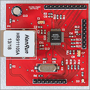
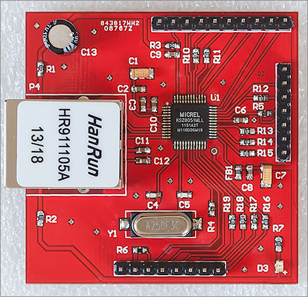
The most significant change is that the RJ45 jack has changed from the TE 6605424-1 to the HanRun HR911105A. The TE connector that I was using is now discontinued so I looked around for a suitable replacement that would be cost-effective and easy to find online.
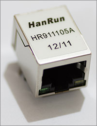
A further advantage of the HanRun device is that the two activity LEDs are built in, saving a few external components on the board itself. The physical footprint of the Hanrun connector is the same as that of the TE with the addition of the extra pins for the LEDs.
It would be nice if there was a standard for the pin assignments on the RJ45 that placed the critical TX+/TX- and RX+/RX- differential pairs right next to each other so that board designers could just route those signals in a straight line. Unfortunately there is no such standard and so we end up having to route those differential pairs in a sub-optimal way.
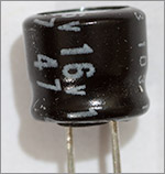
The SMD electrolytic capacitor used for low-frequency decoupling has been replaced with a through-hole model. The through-hole models are cheaper and occupy about the same amount of board-space.
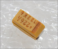
Two of the larger 22µF ceramic decoupling capacitors have been replaced by tantalum devices. At this size tantalum devices are cheaper and just effective as ceramics. Be careful when aligning tantalum capacitors because, like electrolytics they are polarised. The end with the bar drawn across it indicates positive.
The section of the bottom ground plane used for the RJ45 chassis and magnetics is redesigned slightly to ensure that its path to the board’s ground connector keeps it away from the PHY IC.
Schematic
The schematic has been updated to reflect the changes documented above.
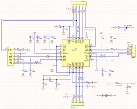
Click the thumbnail for a full-size PDF
Bill of materials
| Identifiers | Value | Footprint | Description |
|---|---|---|---|
| C1,C7 | 22µF | 1206 | Tantalum capacitor |
| C2,C3,C6,C8,C9,C11,C12 | 100nF | 0603 | Ceramic capacitor |
| C4,C5 | 30pF | 0603 | Ceramic capacitor |
| C10 | 2.2µF | 0603 | Ceramic capacitor |
| C13 | 47µF | Radial 2x6x6 | Electrolytic capacitor |
| D3 | red | 0603 | Power LED |
| FB1 | 0603 | Ferrite bead | |
| P1 | 1×10 way | 2.54mm | header |
| P2 | 1×7 way | 2.54mm | header |
| P3 | 1×8 way | 2.54mm | header |
| P4 | HR911105A | RJ45 | Ethernet connector |
| R1,R2 | 220Ω | 0603 | Resistor |
| R3 | 10kΩ | 0603 | Resistor |
| R4 | 6.49kΩ | 0603 | Resistor |
| R5 | 4.7kΩ | 0603 | Resistor |
| R6 | 1kΩ | 0603 | Resistor |
| R7 | 330Ω | 0603 | Resistor |
| R10-R19 | 33Ω | 0603 | Resistor |
| R20 | 0Ω | 0603 | Resistor |
| U1 | KSZ8051MLL | TQFP-48 | Ethernet PHY |
| Y1 | TXC HC-49S-9C 25MHz | custom | Crystal oscillator |
The table above shows the full Bill of Materials for this design. I think all of the components are easy enough to source from the usual online suppliers. I usually use Farnell for my orders. The exception is the HanRun RJ45 connector, these are available for about £1.20 on ebay in single units.
Micrel’s application notes recommend that a ferrite bead be included between the digital and analog supplies (FB1 in this schematic) but they don’t tell you a suitable value. I chose to use the Murata BLM18PG221SN1D which has a low 0.1Ω DC resistance.
You can use a 25MHz crystal oscillator from any manufacturer as long as it fits the same footprint as the TXC HC-49S-9C that I chose. Note that the values for C4 and C5 are dependent on the load capacitance of the crystal. I give the formula that I use to choose these capacitors in the original article.
R20 can be a solder bridge if you don’t have any 0Ω ‘resistors’ to hand. It just connects together the two ground planes. The presence of this bridge as a discrete component in the design is really a hack to work around a limitation in the design software that will not allow you to overlap two polygons that are connected to different net names.
PCB layout
The design still fits within a 50mm square.
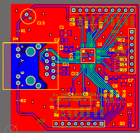
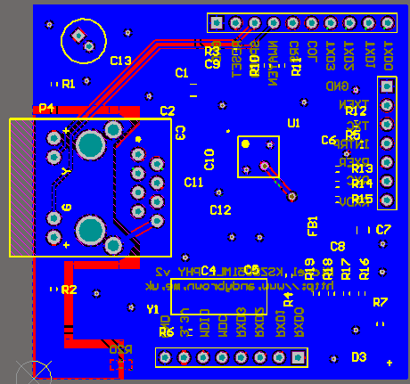
The main difference from the previous design is the change to the ground planes on the bottom layer and the additional routing to reach the LED terminals in the RJ45 connector. You can download the Gerber files for this design from my downloads page.
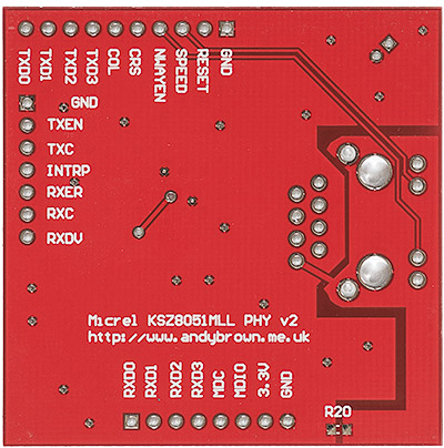
There’s a ground pin on each of three header rows. If you can, connect all of them back to your MCU board but if you’re short of ground pins then at least connect the one that’s on the row containing RXD[0..3].
Return currents follow the path of least impedance back to ground and so it makes sense for the ground pin closest to where the RJ45 ground connections are located to be connected back to the power supply ground on your MCU board. This should keep any noise from the transformer magnetics in the RJ45 from interfering with the PHY.
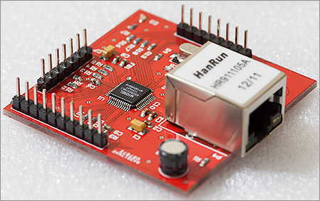
Building the board
With the board now fully routed and the gerber files generated I went ahead and ordered a batch of 10 from Elecrow. Similar services are available from Seeed Studio and ITead Studio but I chose Elecrow this time around because they offer coloured PCBs at no extra cost. I’m almost certain that all these companies are using the same fabrication house.
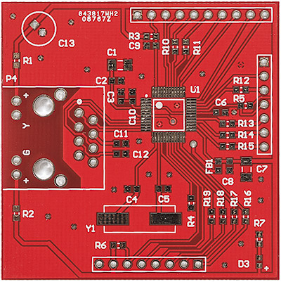
With all the parts to hand I assembled the board by first reflowing the KSZ8051MLL and the oscillator using my hotplate. Next the discrete surface mount components are reflowed using my hot air gun and finally the through-hole components are soldered into place using a normal soldering iron.
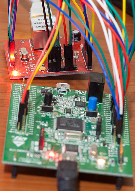
Testing with an MCU
Now the board’s built of course I need to test it. Confidence was high in the workshop that this design would work because it’s an incremental set of improvements over the previous design. Really the only thing that could go wrong was if I’d managed to mis-read the pinout of the Hanrun connector.
I hooked it up to my WaveShare ‘Port107V’ STM32F107 development board and connected the MAC MII pins in the correct manner. The following table shows the MII pinout that I used for the test.
| Pin | Function |
|---|---|
| PC3 | TXC |
| PB12 | TXD0 |
| PB13 | TXD1 |
| PC2 | TXD2 |
| PB8 | TXD3 |
| PB11 | TXEN |
| PA1 | RXC |
| PD9 | RXD0 |
| PD10 | RXD1 |
| PD11 | RXD2 |
| PD12 | RXD3 |
| PB10 | RXER |
| PD8 | RXDV |
| PA0 | CRS |
| PA3 | COL |
| PC1 | MDC |
| PA2 | MDIO |
To test the board I ran the net_udp_send example that is included with my stm32plus C++ library for the STM32 family of microcontrollers.
stm32plus uses a modular C++ TCP/IP stack written by myself and optimised for the MAC included in the larger STM32 devices.
Declaring the physical and datalink layers of the TCP/IP stack to use the KSZ8051MLL with the pinout in the above table is as simple as this:
typedef PhysicalLayer<KSZ8051MLL> MyPhysicalLayer;
typedef DatalinkLayer<MyPhysicalLayer,RemapMiiInterface,Mac> MyDatalinkLayer;
I ran the example and was happy to note that it worked first time. The ethernet link was automatically established and the DHCP client component in the stack successfully obtained IP address details from my router and the example proceeded to send out UDP packets.
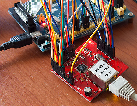
I left it running for a while to ensure that the adaptor was stable. There were no problems so I can happily say that the design is a success.
Connecting to the F4 Discovery board
Several people have contacted me recently to ask if it’s possible to connect this PHY to the STM32 F407 Discovery board, probably the most popular F4 development board out there.
The F4 discovery schematic is freely available and if we examine it then we can see several reasons why it should not work.
- The discovery board runs on 3.0V and the minimum PHY power supply is 3.135V.
- The discovery board maps pins PB10 and PC3 to the CLK and DOUT pins on the MP45DT02 peripheral. PB10 and PC3 are required for MII and cannot be mapped to a different location on the 100 pin STM32 package.
So I tried it anyway…
And it worked! I did have some issues with the PHY reliably establishing a link after reset which seemed to improve when I changed from powering the board from 3V/GND on the discovery to 3.3V/GND on a bench power supply.
If you’re not interested in the MP45DT02 peripheral then I suspect reliability could be further improved by disabling it (cut it’s VDD trace) but at least for now it’s good enough for testing and debugging.
Download the gerbers
Want to build your own boards? If you head on over to my downloads page then you can download the gerber files for this board. Upload them to one of the online PCB printing services and you’ll get ten copies for around $10 plus postage.
The bill-of-materials table in this article should give you all the information that you need to source the components necessary to build the board.