Generic Nokia LCD hacking board

Over the course of the last few months I’ve been presenting schematics and PCBs that you can use to attach various Nokia LCDs to popular microcontrollers. Today I’m going to go one step further and present the generic board that I use for hacking any Nokia LCD that happens to have one of the correct connectors.

The schematic

The aim of this project is to do the following:

  • Break out the 24R-JANK-GSAN-TF connector used by all the QVGA LCDs that I’ve reverse engineered on this site such as the Nokia 2730, 6300, N82, N95 8Gb and N93.
  • Break out the Hirose DF23-10 connector used by the Nokia 6100 and 1600.
  • Break out the Hirose DF23-22 connector used by the Nokia 6101 and others.
  • Provide an optional OnSemi NCP5007 LED driver for the backlights that are powered by up to 4 LEDs in series.
  • With those goals in mind, let’s take a look at the schematic. This image is really small. Click on it to download the schematic as a PDF.
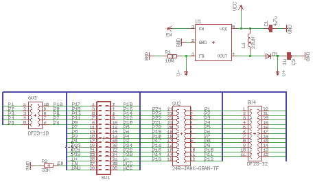


    Click for a PDF

    SV1 is the 0.1″ breakout header. It has up to 24 pins mapped to the Nokia connectors, V+ and V- that correspond to the output and feedback pins for the backlight driver, EN for the backlight driver enable pin, and several VCC and GND pins.

    SV2 is the 24R-JANK-GSAN-TF connector. All 24 pins are mapped to the breakout header.

    SV3 is the Hirose DF23-10 connector. This connector only has 10 pins and so they are mapped to pins P1..10 on the breakout connector.

    SV4 is the Hirose DF23-22 connector. This connector has 22 pins that get mapped to pins P1..22 on the breakout connector.

    Here’s the complete bill of materials for this schematic.

    Part Value Device Package
    SV1 pin header MA15-2 MA15-2
    SV2 Nokia 12×2 24R-JANK-GSAN-TF 12×2
    SV3 Nokia 5×2 Hirose DF23-10 5×2
    SV4 Nokia 11×2 Hirose DF23-22 11×2
    C1 4.7µF ceramic 0805
    C2 1µF 50V ceramic 0805
    D1 CD214A-B140LF Bourns schottky diode DO214AC
    L1 22µH Murata LQH3NP_J0 inductor 1212
    R1 10Ω 1% resistor 0805
    U1 NCP5007 OnSemi LED driver SOT23-5

    The NCP5007 backlight driver is a boost converter that works by continuously raising its output voltage until it overcomes the forward voltage of the LEDs and current starts to flow. It then continues to raise the voltage until the configured current level is detected (I set this to 20mA with a 10Ω resistor in all my designs).

    An important side effect of this design is that the V+ and V- pins must not be left as an open circuit when the device is powered because it will cause the NCP5007 to endlessly raise its voltage output until it either burns out or automatically shuts down. OnSemi, the manufacturer, claims that it has an automatic shutdown for this case but you really don’t want to test that claim.
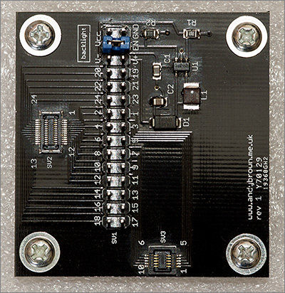
    The PCB layout

    With the schematic design now finalised, I set about designing the PCB.
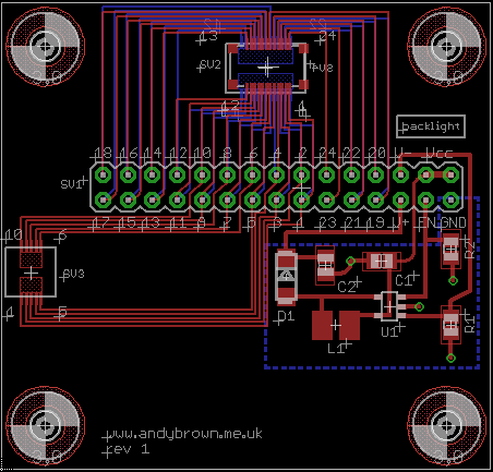


    Click for a PDF

    There wasn’t enough space within the target of 50x50mm to fit all the connectors on the top side so I placed the backlight, breakout, 24R-JANK-GSAN-TF and DF23-10 connectors on the top and the DF23-22 on the bottom.

    Having a connector on the bottom meant that I would need to provide mounting holes for some feet to lift it off my workspace and so there are four 3mm holes provided in the corners.

    Time for manufacturing!

    I use the PCB manufacturing service provided by ITead Studio. After uploading the board to their site it takes between two and three weeks for the finished items to arrive in the mail.

    In a nod to the illicit, underground nature of a reverse engineering board I decided to get them printed with a black solder mask. I know, I need to get out more often.

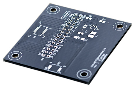
    They look great in black but are nigh on impossible to photograph. I had to hold it at just the right angle to the light to make the features stand out.

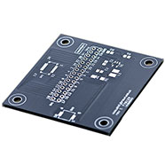
    Here’s an image that shows the front of the PCB with the backlight circuit, 24R-JANK-GSAN-TF and the DF23-10 connectors affixed.

    Pin mappings for popular TFTs

    During the time I spent reverse engineering the various displays I kept notes about the pin mappings. In this section I’ll present those mappings for some of the popular Nokia LCDs.

    In the tables below, ‘board pin’ is the P0..Pn label on my board and ‘schematic pin’ is the pin number on the Nokia schematic found in the repair manual for the corresponding phone.

    Note that these mappings are correct for an LCD connected in the orientation shown in the photograph below.

    6300

    Also known as Connector
    6300, 6301, 5310, 7500, 8600, 6120C, E90 (small), E51 SV2

    Board pin Function schematic pin Notes
    1 LED1- 1 connect to LED2+
    2 LED2- 2 connect to V-
    3 VDDI 3 connect to 3.3V
    4 GND 4
    5 WR 5
    6 D0 6
    7 GND 7
    8 D2 8
    9 D4 9
    10 D6 10
    11 CS 11
    12 RESET 12
    13 TE 13
    14 D7 14
    15 D5 15
    16 GND 16
    17 D3 17
    18 D1 18
    19 RS 19
    20 RD 20
    21 GND 21
    22 VDD 22 connect to 3.3V
    23 LED2+ 23 connect to LED1-
    24 LED1+ 24 connect to V+

    I used the pinout in the above table to connect the board to a Nokia 6300 LCD obtained from ebay. I connected them to an STM32F103VET6 board and ran the mcp2pa8201 demo supplied with my stm32plus library.

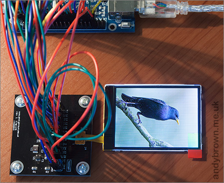
    The above image shows the LCD driven by the STM32 via the hacking board.

    N82

    Also known as Connector
    N79 N78 N77 E66 6210 SV2

    Board pin Function schematic pin Notes
    1 LED- 1 connect to V-
    2 GND 2
    3 VDDI 3 connect to 3.3V
    4 GND 4
    5 WR 5
    6 D0 6
    7 GND 7
    8 D2 8
    9 D4 9
    10 D6 10
    11 CS 11
    12 RESET 12
    13 TE 13
    14 D7 14
    15 D5 15
    16 GND 16
    17 D3 17
    18 D1 18
    19 RS 19
    20 RD 20
    21 GND 21
    22 VDD 22 connect to 3.3V
    23 GND 23
    24 LED+ 24 connect to V+

    N95 8GB

    Also known as Connector
    n/a SV2
    Board pin Function schematic pin Notes
    1 VDD 13 connect to 3.3V
    2 GND 14
    3 TE 15
    4 RESET 16
    5 D1 17
    6 D3 18
    7 D5 19
    8 D7 20
    9 RS 21
    10 RD 22
    11 GND 23
    12 VIO 24 connect to 3.3V
    13 GND 1 labelled KBBC on schematic
    14 GND 2
    15 WR 3
    16 CS 4
    17 D6 5
    18 D4 6
    19 D2 7
    20 D0 8
    21 GND 9
    22 VIO 10 connect to 3.3V
    23 GND 11
    24 VDD 12 connect to 3.3V

    Schematics, CAD and gerbers available

    I have open-sourced my PCB design and CAD files so if you’re interested in building your own boards then head on over to my downloads page and grab yourself a copy.

    Remaining boards for sale

    The remaining blank boards that I have are available for sale at £6.50 for UK delivery and £7.50 for worldwide delivery. Each board includes one 24R-JANK-GSAN-TF connector (unsoldered) to get you started. The boards have the black solder mask, just as pictured in this article.


    Location


  • Erl

    Great work reverse engineering these displays!

    I'm currently modifying a project of mine to use an N95 display, after reading your work.

    Cool board, I might get one.

    A couple of questions:

    * Where do you buy your 24R-JANK-GSAN-TF connectors?

    * Have you tested what voltages the N95 display can run at? I'm wondering if it will run at 3.0V.

    * Have you measured how much current the display uses?

    Regards,

    Erland

    • Hi Erland,

      I got my connectors direct from the JST 'webshop'. To make the shipping and customs fee worthwhile I bought 100 of them.

      I'll bet it runs fine at 3.0V. I think Nokia probably drives them at 2.8V, at least they do on some of the other very similar displays because it's labelled on the repair manual schematic. The LDS285 datasheet quotes a range of 2.3 to 3.3V.

      I haven't measured the current drain. Typically it's very low for the panel itself, less than 10mA depending on refresh rate and other factors. The panel current usage is far outweighed by the consumption of the backlight LEDs (4 white LEDs).

  • Hi,
    thanks for the board:)

    How easy is to use the board with STM32VLDISCOVERY ?

    • If you mean the F100 board then yes you can connect it but you'll need to write a driver to bit-bang the 8080 protocol via the GPIO port. If you mean the F4 discovery board then it's really easy to hook it up to the FSMC peripheral and use it right away with my stm32plus drivers.

      • But will it be to slow that way?

        I also have a F3 discovery. Do your library support it? thanks 🙂

        • GPIO is probably slower than FSMC. I've never tried it on the STM32 so I can't advise on the difference in speed.

          ST certainly have been busy with STM32 releases these days. You get nothing for years and then suddenly they just can't stop releasing them! I don't officially support the F3 yet though I think it's going to be only a slight change from the F4.

          • But compared with the arduino example, do you think that STM32F100 will be faster than arduino? thanks for you help!

          • It'll probably be about the same.

            Using the external memory interface the Arduino can complete a write transaction using an 'sts' instruction in 3 cycles at 16MHz = 187ns.

            Using the STM32F100 you have the advantage of the 16-bit GPIO port that can be used to set up CS, RS, data (x8) and WR (low) in one operation then you need one more operation to bring WR high which triggers the data transfer into the LCD. At a core clock of 24MHz I'd say that should give very similar results to the Arduino.

  • David

    Gread design work!
    I love hacking LCDs too. Last year I found that also the Samsung S5230 LCD is hackable! But still had no time to try.
    It's 400×240 256K colors, and same 8080 parallel interface as nokia ones. It seems to have the S6D04D1 controller.
    This was found on the great LCD hacking post on vrtp.ru
    I'm sure somebody will love this!
    Included in the file: LCD pinout, phone schematic and LCD code for IAR compiler and LPC µController. http://vrtp.ru/index.php?s=46b5ba8731417a33f914f3

    All the credits go to the user srg320 who posted that file here: http://vrtp.ru/index.php?showtopic=1120&st=14

    Nice hacking!

    • Hi David, thank you for your comments. That link is very interesting indeed. I may come back to that and develop something around it at a later date. The connector doesn't look like much fun – it looks like one of those staggered 0.3mm pitch connectors.

      • David

        The connector haA 0.5mm-0.6mm spacing, has 30 pins in dual row (15+15).
        Have a look at the flex that connects the LCD , touch screen and buttons together, it has an unknown 40-pin connector that you can swap with the one on Nokia 5200's flex. That flex also got a male and female matching connector, so its great.

        • David

          Sorry, typo error there. **"The connector has…"

  • Andy
    Other than supplying a JST connector, are the boards completely unpopulated?
    Thanks
    Tom

    • Hi Tom, that's correct they are unpopulated.

  • Erl

    Thanks for the board & connectors.

    Is the 24R-JANK-GSAN-TF connector symmetric? That is, can it be soldered in either orientation? It looks symmetrical in the data sheet, but your PCB layout in the post looked unsymmetrical with wide/narrow traces on the top layout.

    I realize the connector must be plugged in in one specific way.

    Any other tips for soldering the connector?

    Thanks!

    • It is definitely symmetric. I made the Eagle footprint before I knew what the connector was so it won't exactly match the datasheet. In particular I gave myself longer pads so I'd have a little more room to get solder on to them. You can extract my footprint from any of the Nokia LCD schematics in my download section.

      I fix the connector by heavily fluxing the pads and then tinning them with solder. Then I use a small amount of flux as 'glue' to hold the connector in place then I use a hot plate to reflow the connector down on to the pads. After that I put it under the microscope and touch up each pin with a very fine soldering iron and yet more flux.

      If you don't have a hot plate then it is conceivable that you could fix it down with just an iron if you can get it in place and hold it down very firmly while you attach one corner. The pins are quite resilient and are unlikely to bend but the plastic will melt if you touch it with an iron or apply hot air from a reflow station.

  • Erl

    Ok, I think I got it soldered (using an iron. Definitely a challenge for a beginner at surface mount soldering).

    If I understand it correctly, the N95 8GB screen (connector pinout as in the photo on your N95 8GB page) will lie on top of the prototyping board, with the flex cable running over the SV1 connector pinout, is this correct? It seems a bit inconvenient.

    I'm thinking my options are either to turn the prototyping board upside down, and have the connectors on the back, which won't let me see the nice pin numbering, or plugging in the screen the 'wrong way' and having the pin numbers swapped around.

    Any comments or suggestions?

    • Hi Erl, great news that you've got it soldered down.

      I always connect the LCD in the orientation shown in the photograph and the pin mappings in the tables reflect that.

      e.g. for the N95-8Gb, with it connected just like the 6300 in the photograph, you would then connect board pin #1 to VDD, #2 to ground, #4 to RESET etc…

  • Ric

    Thanks indeed for the pinout of Nokia 6300, because it is the same LCD as Nokia 3120c and Nokia 6555, and I have 3 of this phones at home as defective (hope some LCD will live again).
    I had found the Hirose for this LCDs here: http://gsmserver.com/shop/spares/connectors/conne
    But they have out stock the Hirose DF23-22 (I also have 2 Nokia 6085 phones dead).
    Please, where did you buy this Hirose DF23-22 connector to UK ?
    And also a suggestion. STM32F103 has been improved by STM32F205 or STM32F207 in performance.
    STM32F2 models bring true speed of more than 100 Mhz and single cicle instruction real speed.
    They are in the market for a bit more than a year and price is not much higher than STM32F1 models.
    STM32F1 models had program speed lower than clock speed, but ST has made that possible with F2 models.
    Thanks for your wonderful work

  • srinivas

    Hi,

    I have arduino and the nokia n95 LCD panel (expert disassembler, have very basic knowledge on electronics, but no soldering and designing skills). Its amazing how you soldered the smt components and small pins. I wish to buy one finished break out board. please email me

    vsrinu26f at yahoo dot com

    Thanks much for sharing the information.

    • Hi, thank you for your comment. All boards have been sold but you can always build your own. If you go to my downloads page you can download the gerber files for the N95 board. All you need to do is upload these to ITead or Seeed and they'll send you 10 copies for about US$10.

  • Nicholas

    Hi Andy, I'm building this board: Thanks very much for making it an open design! I just sent your gerbers to itead everything's come back looking great.

    One minor note: you missed R2 in your BOM. From the schematic it's 33K, is that right?

    • Hi Nicholas,

      R2 is just a weak pulldown so anything in the 10-60K-ish range is probably fine. I labelled it 33K in the schematic and in practice I'll pick whichever value I've got available in the correct range. Glad you're finding the open design useful. I plan to open source all my designs so that people can learn and experiment on their own.

      Regards,
      – Andy

  • albertteng

    hi, just asking. can we just use a voltage divider? to lower 5v to 3v.

    • Hi Albert, Yes I think so. You'll need a divider for the supply and one each for every signal line. Quite a lot of resistors but it should work. My only concern would be the effect of the resistors on the rise and fall times of the signals but you can experiment to see what's acceptable.

  • Adi

    Why did you not include the level converter in this board?

    • Hi Adi,

      Mainly PCB space on the 5×5 template, also because the main MCU that I use with this design is the 3.3V STM32 which is directly compatible with most of the panels.

  • Hi, Andy!
    Thanks a lot for Your great job!
    I've found Your set of posts while googling info about connecting an LCD to a Raspberry Pi.
    I think this can be done – whats Your opinion?
    There is a linux fbtft project, I suppose the LCD can be driven directly using parallell bus or (to save some GPIO-s) through SPI circuit: https://github.com/notro/fbtft/wiki/SPI-interface
    Waiting for my 24R-JANK- GSAN-TF connector to come (baught on a polish online auction) I'm starting making a prototype PCB 😉
    Thanks again
    Pawel

    • Good luck with the project Pawel. I have no experience with the Pi but it looks like a powerful board so if you have sufficient IOs and low level control over the timings then it should be fine.

  • G.H.Q.D

    Have you ever hack any Nokia touch LCD? 🙂

    • Hi, no I haven’t hacked any touch screens at all.

  • rodrigo ratan

    Great work on hacking the nokia display! Can you confirm if it Works with Nokia C3 LCD, a popular Nokia Asha phone on emerging markets like Brazil?

    • Sorry Rodrigo but I have no experience with the C3.

  • Ryan

    Wow….. nice project, is it possible to run the nokia 9300 / 9300i lcd (640X200) with arduino 2560?

    Thanks

    • Sorry but I have no experience with that phone.

      • Ryan

        Ok, Thanks

  • Ryan

    Wow….. nice project, is it possible to run the nokia 9300 / 9300i lcd (640X200) with arduino 2560?

    Thanks