


stm32plus 3.2.0: Supporting the STM32F0 Cortex M0
A few months ago I made the decision to start supporting the lower priced, hobbyist friendly STM32 devices in my stm32plus C++ library. These lower-end devices come in lower pin-count, smaller packages that are easier to work with and they have reduced clock speeds that make for fewer PCB layout headaches.
The first low-end STM32 series to be supported was the medium density ‘value line’ F1 (Cortex M3) as exemplified by ST’s Value Line Discovery board. This was supported in stm32plus 3.1.1. Now with release 3.2.0 stm32plus is supporting the STM32F0 (Cortex M0) series of MCUs.
About the STM32F0
The STM32F0 is an implementation of the 32-bit ARM Cortex M0 core. The Cortex M0 core is very similar to that of the M3 and M4 except that some of the instructions and addressing modes are not present. This is not something that you will notice as a C++ programmer but it does impose limitations if you like to dabble in assembly language now and then.
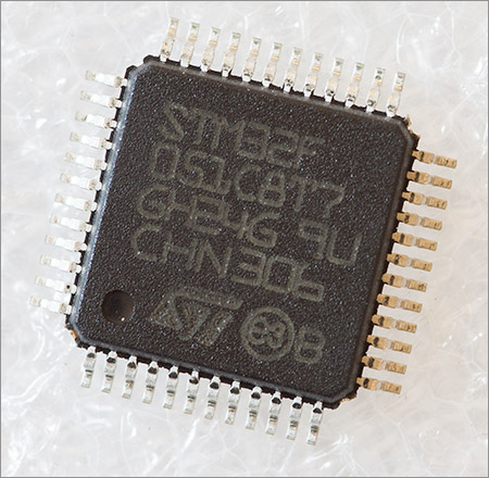
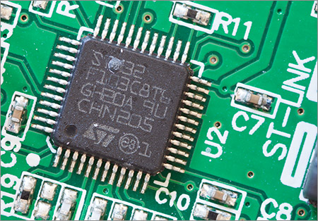
The device in the picture is the STM32F051C8T7. At the time of writing this MCU costs £2.60 plus tax from Farnell in single units. For that you get a 48MHz core with 64Kb of flash and 8Kb of SRAM in an LQFP package that does not require an external oscillator, thereby saving even more off the total design cost. This compares very favourably with similarly resourced 8-bit MCUs from companies such as ATmel.
The same flat 32-bit address structure is present on the M0 with the flash memory, SRAM and peripheral registers all mapped in to the usual address regions. If you’ve programmed the Cortex M3 or M4 then you’ll be right at home with the M0.
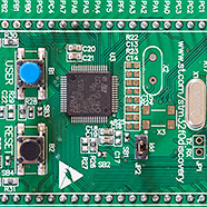
ST provide a very low cost development board for the M0 in the ‘discovery’ range.
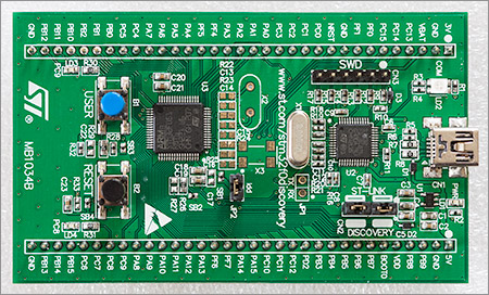
The STM32F0 Discovery comes with an STM32F051R8T6 on board as well as an ST-Link v2 USB debugger interface. It’s on sale from Farnell at the moment for £6.78 plus tax.
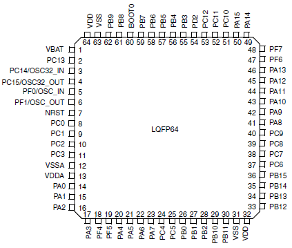
The diagram above shows the pinout of the LQFP64 package included on the F0 discovery board. The 16-bit GPIO ports A, B and C are included in their entirety with a few pins each from ports D and F.
There’s a very important warning buried deep inside reference manual RM0091 that applies to GPIO ports PC13 to 15. It’s well hidden in the power control (PWR) section and I’m going to quote it here because you need to know this.

|
Due to the fact that the analog switch can transfer only a limited amount of current (3 mA), the use of GPIOs PC13 to PC15 in output mode is restricted: the speed has to be limited to 2 MHz with a maximum load of 30 pF and these IOs must not be used as a current source (e.g. to drive an LED). |
I produced a quick video that walks you through the STM32 F0 Discovery board, click on the embedded player below to watch it or click here to watch it in HD on YouTube.
http://youtu.be/TCXGuYDWuv0
stm32plus support
The M0 support in stm32plus is generic enough that it should work on all of the M0 devices, however I did the development against the F0 discovery board so support is officially for the F051 series. All of the examples target the F051 at 48MHz with 64Kb flash, 8Kb SRAM and running off the internal 8MHz oscillator (HSI).
Assuming that you’ve downloaded and extracted the source code archive from github then you can build the library and all the compatible examples from a terminal prompt:
scons mode=debug mcu=f051 hse=8000000 -j4
Some notes on the above command:
- Even though the examples use the 8MHz HSI oscillator you still need to supply a value for the
hseparameter. 8000000 is a suitable default value. - You need to have installed
sconson your system. Consult your package management system for the exact installation syntax. On Ubuntu it would besudo apt-get install scons. - Windows users must use a Unix-alike subsystem such as Cygwin or msys. I use Cygwin on Windows 7 x64.
- Where I have used the
mode=debugoption I could also have usedsmallorfastmode options to build the library optimised for size or speed, respectively. - The parameter to the
-joption should reflect the number of cores in your build system.
OpenOCD and the ST-Link V2 debugger
Interactive debugging using the Eclipse CDT edition does not need any additional hardware because there is an ST-Link chip built on to the board. It’s interesting to note that ST have implemented the ST-Link interface using an STM32 F103 MCU.
To drive the ST-Link you need to get a copy of the freeware OpenOCD utility. At the time of writing the latest version is 0.7.0 and the source can be downloaded from Sourceforge.
If you’re not interested in building from source then Linux users can install it using their package manager, e.g. for Ubuntu it would be sudo apt-get install openocd.
Windows users can download compiled binaries from this location.
OpenOCD runs in the foreground as a server process so you need to fire up a terminal window and run it with the appropriate options. I like to create trivial scripts that I can use to start OpenOCD on demand. For example, this is my script for Windows 7 x64 on Cygwin:
#!/bin/sh

cd openocd-0.7.0
bin-x64/openocd-x64-0.7.0.exe -f scripts/board/stm32f0discovery.cfg
If it’s all working then you should see output like this when you run OpenOCD:
Open On-Chip Debugger 0.7.0 (2013-05-05-10:44)
Licensed under GNU GPL v2
For bug reports, read
        http://openocd.sourceforge.net/doc/doxygen/bugs.html
srst_only separate srst_nogate srst_open_drain connect_deassert_srst
Info : This adapter doesn't support configurable speed
Info : STLINK v2 JTAG v14 API v2 SWIM v0 VID 0x0483 PID 0x3748
Info : Target voltage: 2.888784
Info : stm32f0x.cpu: hardware has 4 breakpoints, 2 watchpoints
At this stage OpenOCD is running as a server and you can either telnet to it and issue direct commands or you can use Eclipse to flash the board and do some visual debugging. Let’s first look at directly sending commands to it using a telnet session.
Controlling OpenOCD with telnet
Here’s a log of a real telnet session to OpenOCD.
$ telnet localhost 4444
Trying 127.0.0.1...
Connected to localhost.
Escape character is '^]'.
Open On-Chip Debugger
> reset init
target state: halted
target halted due to debug-request, current mode: Thread
xPSR: 0xc1000000 pc: 0x08000aec msp: 0x20002000
> flash write_image erase p:/stm32plus-examples-blink.hex
auto erase enabled
device id = 0x20006440
flash size = 64kbytes
wrote 3072 bytes from file p:/stm32plus-examples-blink.hex in 0.531030s (5.649 KiB/s)
> reset
Let’s take a look at what’s going on here. Firstly I use telnet to establish a session with OpenOCD:
telnet localhost 4444
OpenOCD responds with a one-liner greeting and a simple > prompt. The first thing I need to do is to reset the board and halt it so that I can flash my program.
reset init
OpenOCD logs the fact that the MCU was reset and is now halted awaiting my next command. I will now flash the board with an ihex file that was produced when I built the stm32plus package and all its examples.
flash write_image erase p:/stm32plus-examples-blink.hex
OpenOCD logs its progress and eventually tells me that it’s written 3072 bytes to the MCU. The device is still halted so now I’m going to reset it and this time let it go so my program will run.
reset
The program is now running and the onboard LED is blinking at a rate of 1Hz.
Controlling OpenOCD with Eclipse
If you’re using Eclipse to do your development then you can have all the OpenOCD interaction automated by the gdb debugger and you’ll get visual debugging with breakpoints and variable/memory inspection. Pretty much everything you’d expect to get from a PC-based debugger.
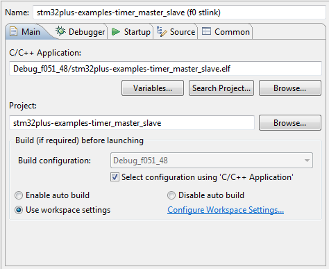
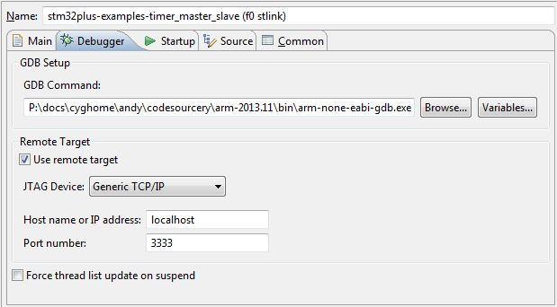
Assuming that you’ve got a project that builds and produces a .elf file as its output, open the Run -> Debug Configurations form and create a new GDB Hardware Debugging configuration for your project.
All the important options are on the first three configuration tabs. Rather than list them all by rote I’ll show some screenshots of one of my configurations. It should be easy for you to adapt these details to your project:
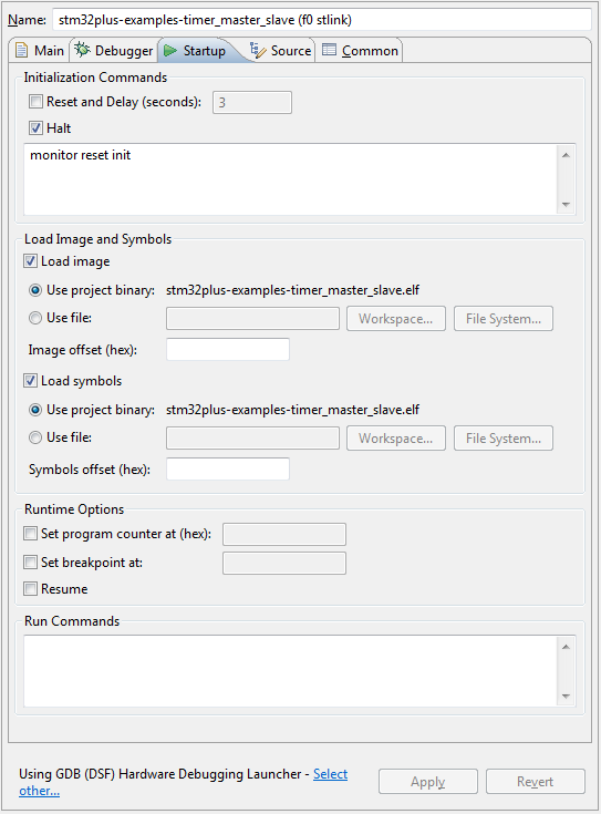
Now when I launch this configuration the latest build of the project will be automatically flashed to the board and it will reset and halt. I can then use the Resume Eclipse command to start the program.
Finally
Support for the F0 is now a core feature of stm32plus and will be maintained accordingly in each release. I’ve got a project or two in mind that will use the F0 MCU and of course those projects will be written up here on this website as they come to fruition.